Plasma display device and method for driving the same

Inactive Publication Date: 2005-03-31
PANASONIC CORP
View PDF3 Cites 31 Cited by
  • Summary
  • Abstract
  • Description
  • Claims
  • Application Information

AI Technical Summary

Benefits of technology

[0028] In view of the above, it is an object of the present invention to provide a plasma display device which is capable of avoiding erroneous operations and of performing stable operation

Problems solved by technology

If writing on a following line is done in a state in which wall charges formed by the discharge occurred during the sustaining period 1 in the previous sub-field are still left, due to influences caused by the left wall charges being different depending on a lighting state of a cell in the sustaining period 1, occurrence of smooth writing discharge is made difficult, thus causing erroneous writing.
In particular, if an amount of wall charges and/or an amount of space charges are changed in the initializing period, a writing discharge state during the scanning period thereafter varies which, therefore, causes erroneous non-lighting or erroneous lighting.
The self-erasing discharge is intense discharge and, if the initializ

Method used


Image

  • Plasma display device and method for driving the same
  • Plasma display device and method for driving the same
  • Plasma display device and method for driving the same

Examples


first embodiment

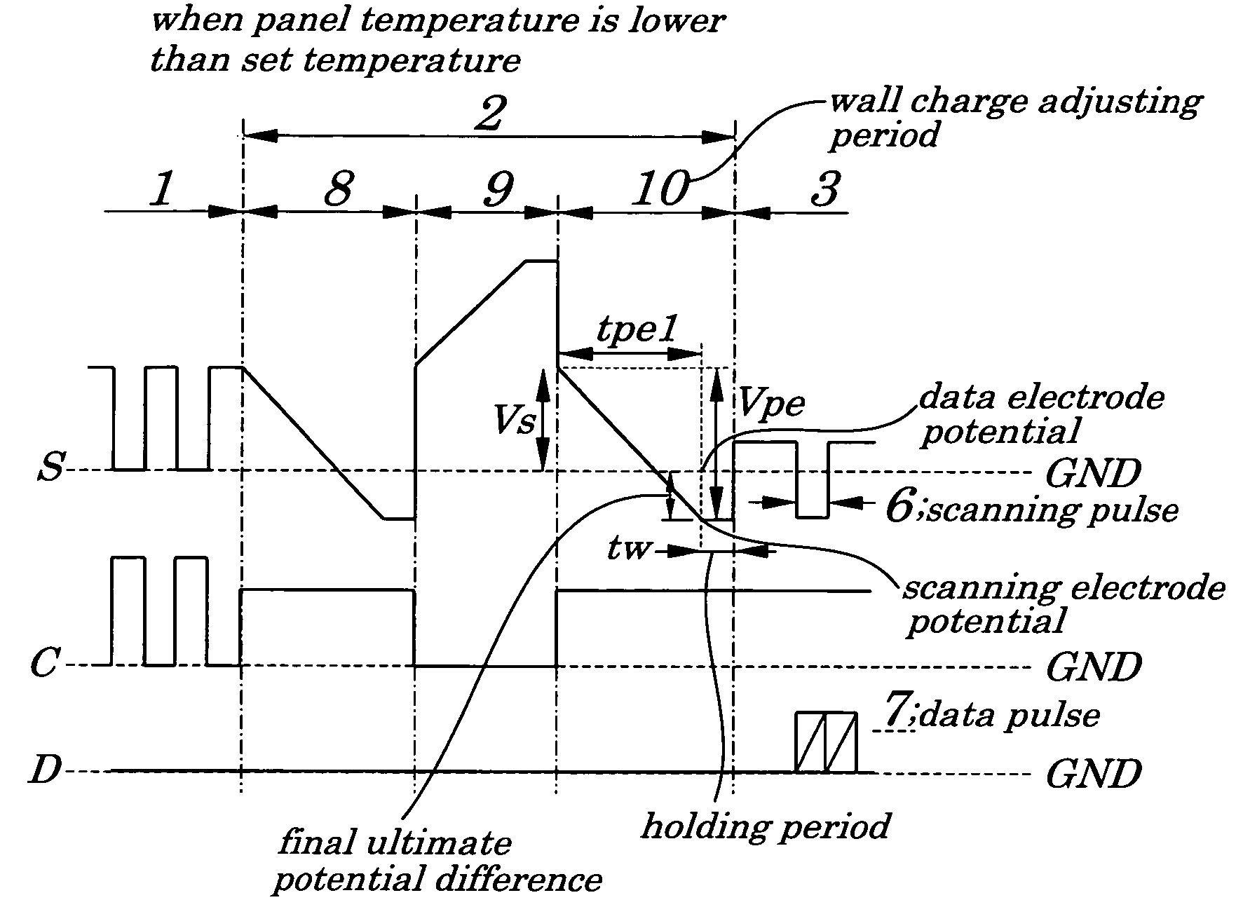
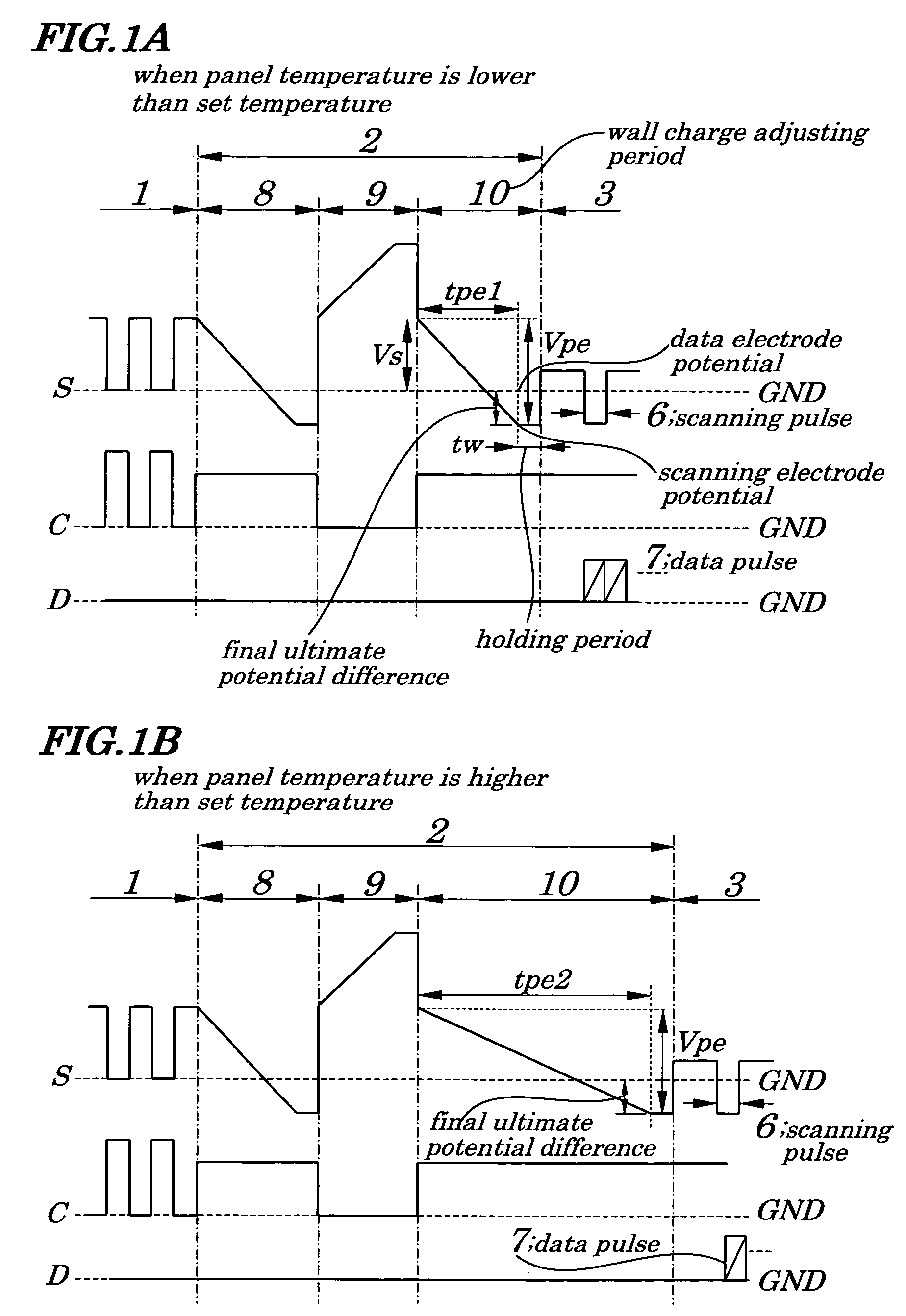
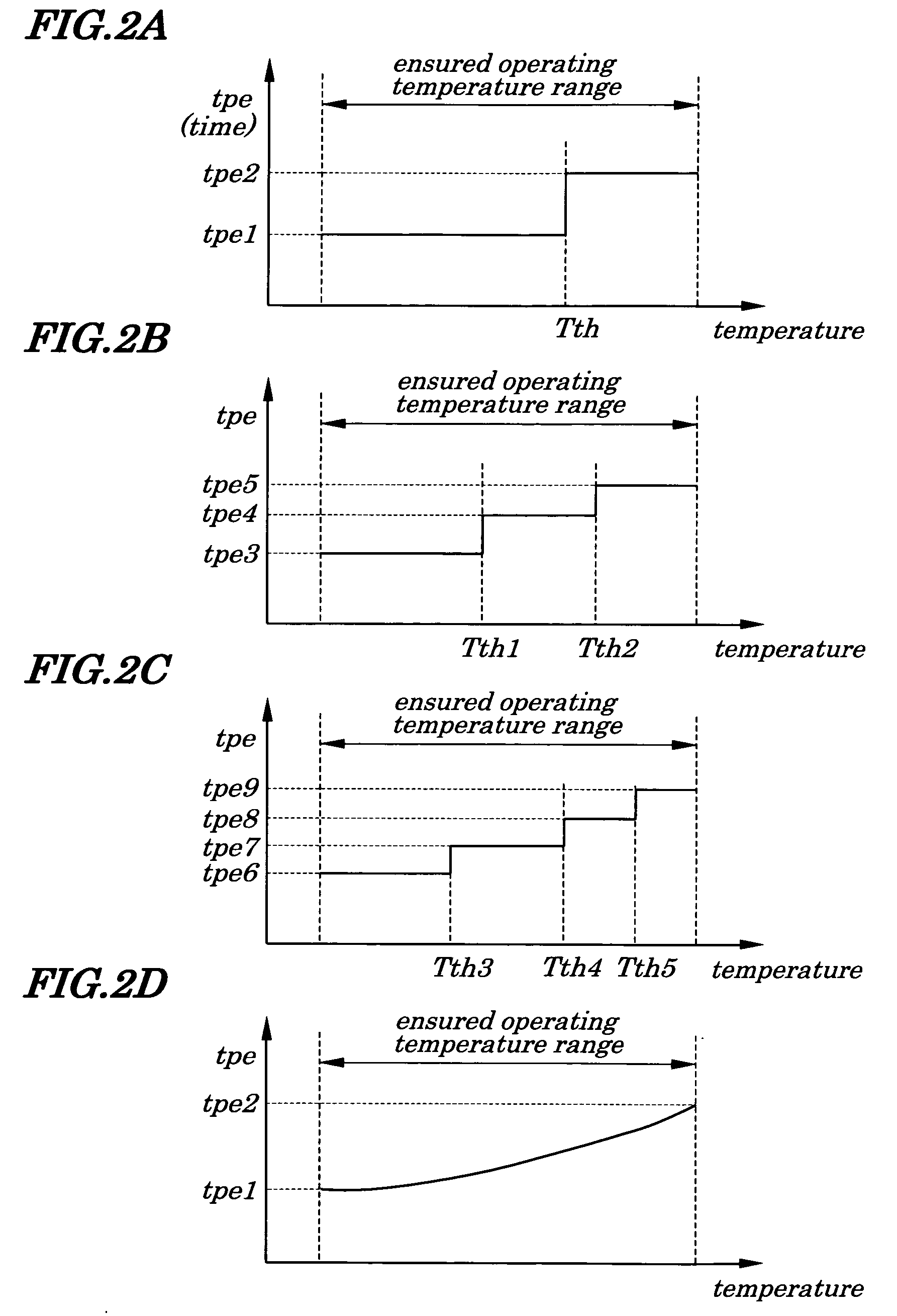
[0087]FIGS. 1A and 1B are diagrams showing driving waveforms of pulses applied immediately before, after, and during an initializing period in a PDP used in a plasma display panel of a first embodiment of the present invention. FIG. 2A is a diagram showing a relation between time and temperature in a period during which a voltage changes during the wall charge adjusting period in the plasma display panel of the first embodiment. FIG. 3 is a diagram showing temperature dependence of minimum and maximum data pulse voltages required for normal operations of the PDP used in the plasma display device of the first embodiment. The PDP being used in the plasma display device of the first embodiment is the same as the conventional one shown in FIGS. 17 and 18 and their descriptions are omitted accordingly.

[0088] In the plasma display device of the first embodiment, in order to measure a panel temperature of the PDP, a temperature sensor is attached on a driving substrate in a rear of the pa...

second embodiment

[0100]FIGS. 4A and 4B are diagrams showing configurations making up one field employed in a PDP respectively for the first and second embodiments of the present invention. FIGS. 5A and 5B are diagrams showing driving waveforms of pulses applied, when a panel temperature is lower or higher than a set temperature, immediately before, after, and during an initializing period in the PDP used in the plasma display device of the second embodiment of the present invention. The configurations of the PDP being used in the plasma display device of the second embodiment are the same as those of the conventional one shown in FIGS. 17 and 18. In the second embodiment, as in the first embodiment, a temperature sensor is attached on a driving substrate in a rear of a panel so as to measure the panel temperature.

[0101] The method for driving the PDP of the second embodiment is the same as that employed in the first embodiment except that, in the driving waveforms of pulses to be applied when the p...

third embodiment

[0108]FIG. 2B is the diagram showing the relation between time and temperature in a period during which a voltage changes during wall charge adjusting period in the third embodiment of the present invention. FIG. 6 is a diagram showing temperature dependence of maximum and minimum data pulse voltages required for normal operations of the PDP used in the plasma display device of the third embodiment of the present invention. The configurations of the PDP being used in the plasma display device of the third embodiment are the same as those of the conventional one shown in FIGS. 17 and 18. In the third embodiment, a temperature sensor is also attached on a driving substrate in a rear of a panel so as to measure a panel temperature.

[0109] In the method for driving the PDP of the third embodiment, as shown in FIG. 2B, basic configurations of driving waveforms of applied pulses and operations for changing a change rate of a scanning electrode voltage during the wall charge adjusting peri...


PUM


Abstract

A plasma display device is provided which is capable of expanding an ensured operating temperature range or operating life time even at time of changes of a driving margin induced by a panel temperature or cumulative operating time of the panel. Display is controlled in a scanning period during which writing discharge is made to occur in a cell, in a sustaining period during which a cell having undergone writing discharge is turned ON for displaying, and in an initializing period during which wall charges in a cell and space charges accumulated before the scanning period starts are initialized. A wall charge adjusting period during which a potential difference between scanning electrodes and data electrodes varies gradually is set and a change rate of a potential between scanning electrodes and data electrodes during the wall charge adjusting period is changed according to the panel temperature and/or cumulative operating time of the panel.

Description

BACKGROUND OF THE INVENTION [0001] 1. Field of the Invention [0002] The present invention relates to a plasma display device having a three-electrode AC (Alternating Current) type of plasma display panel and a method for driving the plasma display device. [0003] The present application claims priority of Japanese Patent Application No. 2003-307915 filed on Aug. 29, 2003, which is hereby incorporated by reference. [0004] 2. Description of the Related Art [0005] A plasma display panel (hereinafter may be referred to simply as a “PDP”) has, in general, many advantages in that it can be made thin, display on a large screen is made possible with comparative ease, it can provide a wide viewing angle, it can give a quick response, and a like. Therefore, in recent years, the PDP is being widely and increasingly used, as a flat display panel, for wall-hung TVs, public information boards, or a like. The PDP is classified, depending on its operating method, into two types, one being a DC (Dire...

Claims


Application Information

Patent Timeline
IPC IPC(8): G09G3/20G09G3/288G09G3/291G09G3/292G09G3/293G09G3/294G09G3/296G09G3/298
CPCG09G3/2022G09G3/2927G09G2320/041G09G2320/0228G09G2310/066G09G3/292G09G3/296
Inventor MIZOBATA, EISHINAKAMURA, TADASHI
Owner PANASONIC CORP
Why Eureka
Try Eureka