Inter-chip and intra-chip wireless communications systems

Inactive Publication Date: 2005-04-07
NANYANG TECH UNIV
View PDF6 Cites 69 Cited by
  • Summary
  • Abstract
  • Description
  • Claims
  • Application Information

AI Technical Summary

Benefits of technology

[0015] It is also further an objective of the present invention to provide a μ-Satellite capability

Problems solved by technology

Thus the voltage drop across the wire is increasing as well as the

Method used


Image

  • Inter-chip and intra-chip wireless communications systems
  • Inter-chip and intra-chip wireless communications systems
  • Inter-chip and intra-chip wireless communications systems

Examples


Embodiment Construction

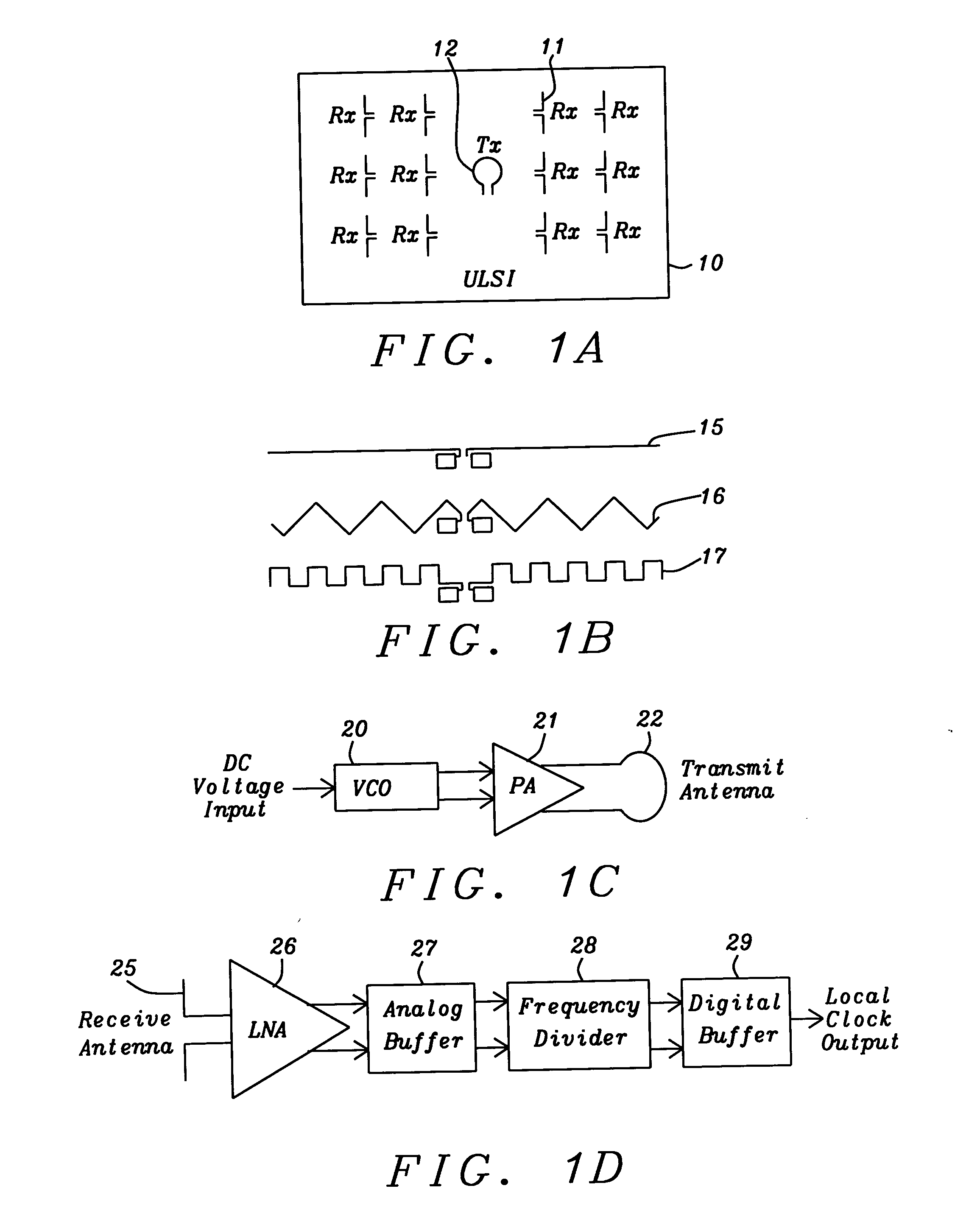
[0037] In FIG. 1A is shown a diagram of a large integrated circuit chip 10 with a plurality of receiving circuits 11 and a transmission circuit 12. The plurality of receiving circuits and the transmission circuit are represented by symbols of antennas. In this configuration one sending circuit is communications with a plurality of receiving circuits where the receiving circuits are circuits performing a similar such as is the case with clock signals. FIG. 1 B shows examples of dipole antenna shapes 15, 16 and 17 similar to the shapes that are formed by metallization on the large integrated circuit chip. The length of the antenna is an appreciable amount of a quarter wavelength which requires the frequency of the RF signals that are being transmitted and received to be greater than a gigahertz. The higher the transmitted frequency is, the smaller the wavelength of the propagating RF signal and the shorter the length of the dipole antennas. A preferred frequency of the RF signal is gr...


PUM


Abstract

A method and implementation for communicating between logic functions using non-metallic coupling between logic functions on a same chip or separate chip is shown. For communication on the same chip, radiated energy from an antenna coupled to a transmitting logic function is coupled to a receiving antenna and then coupled by an electrical connection to a receiving logic function. Communication between USLI chips mounted on a module is performed by coupling an RF signal from a first chip to a μ-satellite mounted within the module and then coupling the RF signal from the satellite to a second chip. Communication can also be formed between the satellite and different logical functions on the same USLI chip.

Description

[0001] This application claims priority to Provisional Patent Application Ser. No. 60 / 508,394, filed on Oct. 3, 2003, which is herein incorporated by reference in its entirety.BACKGROUND OF THE INVENTION [0002] 1. Field of Invention [0003] The present invention is related to communication between integrated circuits and in particular inter-chip and intra-chip wireless communications. [0004] 2. Description of Related Art [0005] The advancement in the development of semiconductor devices continues with an improvement in circuit density and performance. To accomplish this there is a reduction in CMOS device size including the width and spacing of the interconnecting metallization. Operating speed and cut-off frequencies of the CMOS devices are increasing and speeds greater than 100 GHz will be realized in the future. The resistance of interconnecting wiring is being maintained by the use of copper wiring, but the total length of wiring is increasing as complete functions are integrated...

Claims


Application Information

Patent Timeline
IPC IPC(8): H01L23/48H01Q1/22H01Q23/00H04B1/40H04B1/69
CPCH01L23/48H01L24/73H01L2924/10253H01L2224/48227H01L2924/01013H01L2924/01029H01L2924/14H01L2924/3011H01Q1/22H01Q1/2283H01Q23/00H04B1/40H04B1/7163H01L24/48H01L2924/01005H01L2924/01006H01L2924/01019H01L2924/01023H01L2924/01033H01L2924/01074H01L2223/6677H01L2924/15311H01L2224/73253H01L2224/16225H01L2924/00H01L2924/16152H01L2924/16251H01L2924/00014H01L2224/45099H01L2224/45015H01L2924/207
Inventor ZHANG, YUE PING
Owner NANYANG TECH UNIV
Why Eureka
Try Eureka