

Developing method, substrate treating method, and substrate treating apparatus
a technology of substrate treatment and treating method, applied in the direction of cleaning using liquids, instruments, photosensitive materials, etc., can solve the problem of pattern density and pattern finishing dimension differences
- Summary
- Abstract
- Description
- Claims
- Application Information
AI Technical Summary
Benefits of technology
Problems solved by technology
Method used
Image

Examples
first embodiment
[0066] (First Embodiment)
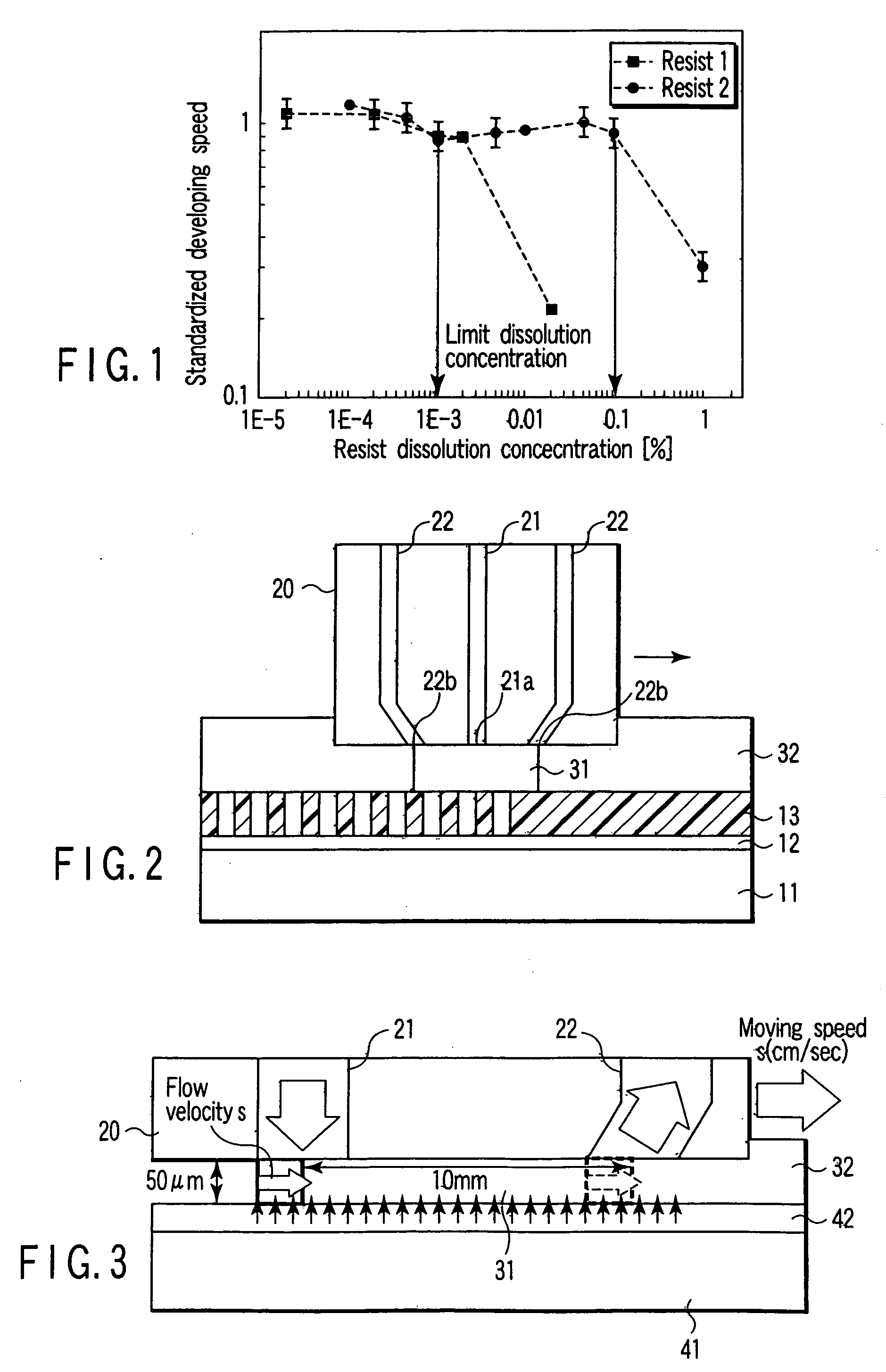
[0067] First of all, changes of a developing speed (dissolving speed) when resist is dissolved in developing solution was experimented at various resist dissolution concentrations. The developing solution used in the experiment was 2.38% TMAH. Results of the experiment are shown in FIG. 1. FIG. 1 is a diagram showing the relation between resist dissolution concentration and developing speed according to a first embodiment of the invention.
[0068]FIG. 1 is a characteristic diagram showing the developing speed in relation to the resist dissolution concentration. In FIG. 1, resist 1 and resist 2 are tested. The developing speed of each resist is standardized by the developing speed in developing solution with the resist dissolution concentration of 0%.
[0069] The resist 1 and resist 2 in FIG. 1 are composed of similar components, but are substantially different in a mode of change of the developing solution in relation to the resist dissolution concentration. A...
second embodiment
[0106] (Second Embodiment)
[0107] A configuration of a solution discharge / suction unit (called scan nozzle hereinafter) of a developing apparatus used in this embodiment will be explained by referring to FIG. 12 to FIG. 14. FIG. 12 is a plan view showing a configuration of the bottom of a scan nozzle. FIG. 13 is a sectional view showing the configuration of the scan nozzle. FIG. 14 is a view of the scan nozzle from the front side in the moving direction.
[0108] The solution discharge / suction unit (called scan nozzle hereinafter) measures about 18 cm in width in a direction perpendicular to the moving direction on the substrate, and 5 cm in depth in a direction parallel to the moving direction. As shown in FIG. 12, there are five slit openings 121 to 125 in the side of the scan nozzle facing the substrate. A developing solution is discharged from the central opening (developing solution discharge slit) 121. A solution on the substrate is sucked from both adjacent openings (suction sli...
third embodiment
[0129] (Third Embodiment)
[0130] In the second embodiment, there is described the developing method for finishing the pattern uniformly by adjusting the gap depending on the ratio of the exposure unit. This embodiment relates to a developing method for finishing the pattern uniformly by adjusting the scan speed of the scan nozzle depending on the ratio of the exposure unit.
[0131]FIG. 21 shows the relation between the average aperture rate after development of a 5 mm square region in positive type resist, and the scan speed of the nozzle for finishing to a desired resist dimension. As shown in FIG. 21, it is found that, as the aperture rate increases, an appropriate scan speed slows down. This is because, as the aperture rate is larger, the volume of resist to be removed increases, and the developing solution must flow a longer time to supply a fresh developing solution by a greater volume. By making use of this relation, an example in which a photo mask is actually manufactured will...
PUM
| Property | Measurement | Unit |
|---|---|---|
| width | aaaaa | aaaaa |
| flow speed | aaaaa | aaaaa |
| thickness | aaaaa | aaaaa |
Abstract
Description
Claims
Application Information