Electro-optical device, color filter substrate, method of manufacturing electro-optical device, and electronic apparatus

a technology of electrooptical devices and substrates, applied in the direction of optics, static indicating devices, instruments, etc., can solve the problems of insufficient luminosity of display images in reflective displays, and insufficient chroma or luminosity of display images in respective displays, etc., to achieve excellent white balance

Active Publication Date: 2005-04-21
BOE TECH GRP CO LTD
View PDF19 Cites 28 Cited by
  • Summary
  • Abstract
  • Description
  • Claims
  • Application Information

AI Technical Summary

Benefits of technology

[0035] As described above, according to the present invention, the planar areas of the transparent layers are different from each other for every colored layer, and thus it is possible to voluntarily change a color balance in the reflective display. Further, in the reflective display, it is possible to adjust the color balance such that the optimum luminosity may be obtained for every color, and thus it is possible to obtain an electro-optical device which has a display property exhibiting an excellent white balance.

Problems solved by technology

Therefore, in the case that the transmissive display and the reflective display use the common colored layers, there is a problem in that chroma or luminosity of display images in the respective displays is lacking.
That is, if the colored layers having low pigment concentrations are used so as to obtain the optimum chroma in the reflective display, the chroma of display images becomes insufficient in the transmissive display.
Meanwhile, if the colored layers having high pigment concentrations are used so as to obtain the optimum chroma in the transmissive display, the luminosity of display images becomes insufficient in the reflective display.

Method used


Image

  • Electro-optical device, color filter substrate, method of manufacturing electro-optical device, and electronic apparatus
  • Electro-optical device, color filter substrate, method of manufacturing electro-optical device, and electronic apparatus
  • Electro-optical device, color filter substrate, method of manufacturing electro-optical device, and electronic apparatus

Examples


example 1

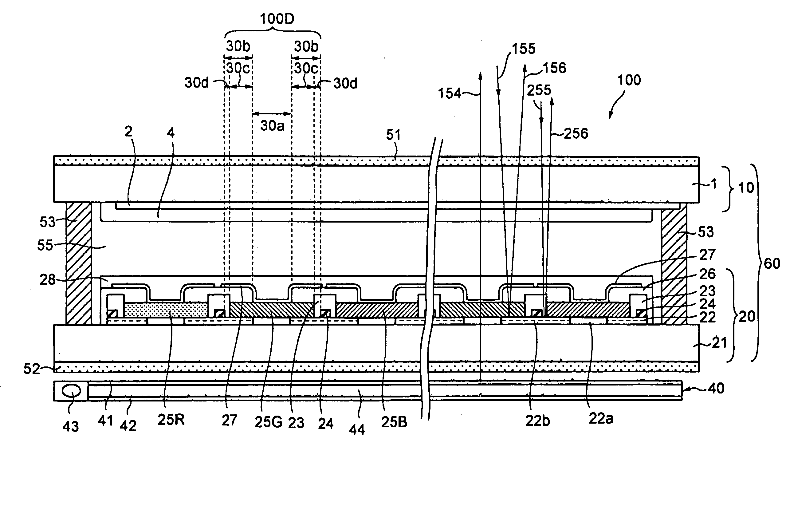
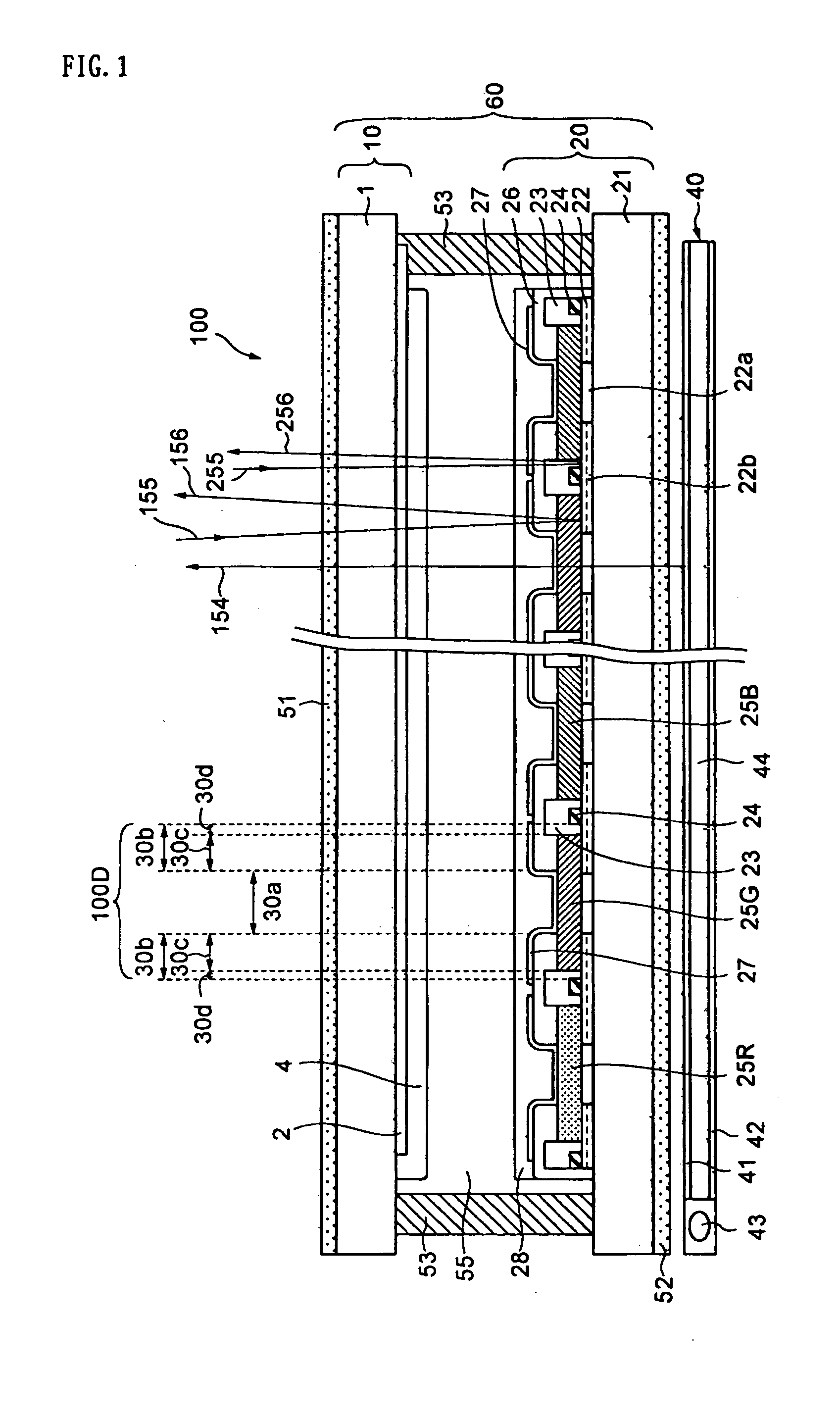
[0061] The color filter substrate 20 in example 1, which is incorporated into the above-mentioned liquid crystal device 100, will now be described in detail with reference to FIGS. 2 and 3.

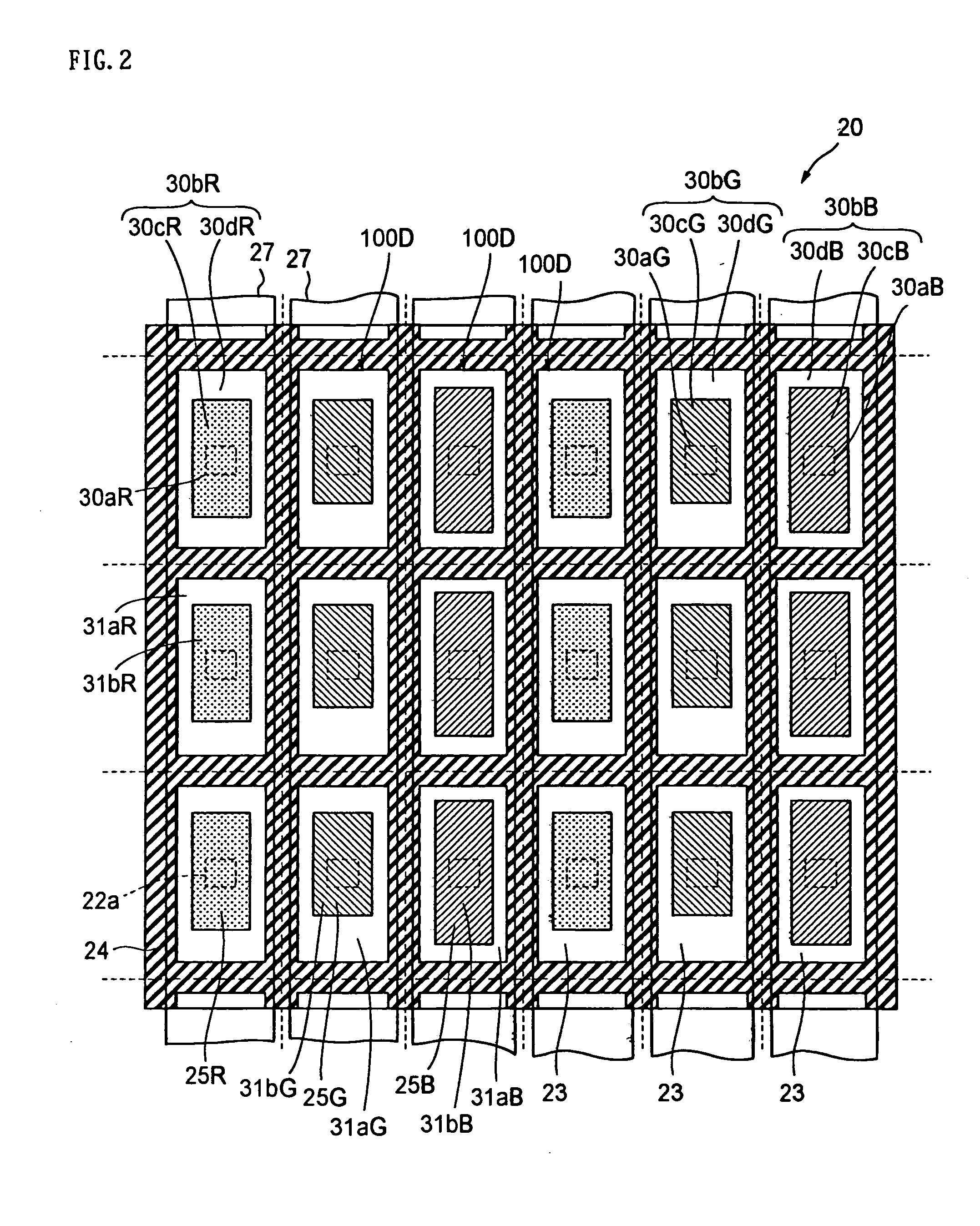
[0062]FIG. 2 is a partial schematic plan view of the color filter substrate 20 constituting a part of the liquid crystal device 100. FIG. 3(a) is a partial schematic plan view of FIG. 2, which corresponds to one pixel. FIG. 3(b) is a cross-sectional view taken along the line A-A′ of FIG. 3(a), in which an alignment film is not shown.

[0063] As shown in FIG. 2, the color filter substrate 20 includes a plurality of dot portions 100D. In a state in which the color filter substrate 20 is incorporated into the liquid crystal device 100, the respective dot portions 100D are formed in correspondence with the positions at which the second electrodes 27 and the first electrodes 2 on the counter substrate 10 opposite to the second electrodes 27 overlap with each other in plan view. Each of the dot portions...

example 2

[0085] In the color filter substrate 20 of example 1, the light-shielding layer is provided, but similar to an example 2 descried below, a structure in which a light-shielding layer is not provided may be configured. The present example will now be described with reference to FIGS. 4 and 5, but the description of the same elements as those of example 1 will be omitted.

[0086]FIG. 4 is a partial schematic plan view of a color filter substrate in example 2. FIG. 5(a) is a partial schematic plan view of FIG. 4, which corresponds to one pixel. FIG. 5(b) is a cross-sectional view taken along the line B-B′ of FIG. 5(a).

[0087] As shown in FIG. 4, a color filter substrate 220 includes a plurality of dot portions 200D. In the color filter substrate 220 of the present example, after it is incorporated into the liquid crystal device, regions that actually contribute to display correspond to the dot portions 200D. That is, in a state in which the color filter substrate is incorporated into the...

example 3

[0094] In the above-mentioned examples, the planar shapes of the bank layer regions in the dot portions are in a frame shape, but similar to a color filter substrate of an example 3 described below, the planar shapes of the bank layer regions in the dot portions may be in an island shape. The present example will now be described with reference to FIGS. 6 and 7, but the description of the same elements as those of example 1 will be omitted.

[0095]FIG. 6 is a partial schematic plan view of a color filter substrate in an example 3. FIG. 7(a) is a partial schematic plan view of FIG. 6, which corresponds to one pixel. FIG. 7(b) is a cross-sectional view taken along the line C-C′ of FIG. 7(a), and FIG. 7(c) is a cross-sectional view taken along the line D-D′ of FIG. 7(a).

[0096] As shown in FIG. 6, the color filter substrate 320 includes a plurality of dot portions 300D. In the present example, as seen from a direction orthogonal to the substrate, the liquid crystal device into which the...


PUM

PropertyMeasurementUnit
colorsaaaaaaaaaa
transparentaaaaaaaaaa
coloraaaaaaaaaa

Abstract

A transflective liquid crystal device is provided that has red, green and blue colored layers provided in correspondence with a plurality of dot portions, and reflective layers overlapping the colored layers in plan view. In the plurality of dot portions, transparent bank layers and colored layers arranged to fill regions defined by the bank layers are respectively provided, and the forming areas of the bank layers in the respective dot portions are different from each other such that the forming areas of the colored layers in the respective dot portion are different for each color.

Description

RELATED APPLICATIONS [0001] This application claims priority to Japanese Patent Application No. 2003-318428 filed Sep. 10, 2003 which is hereby expressly incorporated by reference herein in its entirety. BACKGROUND [0002] 1. Technical Field [0003] The present invention relates to an electro-optical device, a color filter substrate, a method of manufacturing the electro-optical device, and an electronic apparatus. [0004] 2. Background Art [0005] A transflective liquid crystal device as an electro-optical device which combines a reflection type and a transmission type can be switched into one of a reflective display mode and a transmissive display mode according to the surrounding luminosity. In such a liquid crystal device, a reflective layer comprising a reflective portion for reflecting external light and a transmissive portion formed of an opening of a reflective film for every pixel is provided. Thus, when the illuminating means is turned on, illuminating light passes through the...

Claims


Application Information

Patent Timeline
Patent Type & Authority Applications(United States)
IPC IPC(8): G02B5/20G02F1/133G02F1/1335
CPCG02F1/133555G02F1/133514G02F1/1335
Inventor NAKANO, TOMOYUKITAKIZAWA, KEIJI
Owner BOE TECH GRP CO LTD
Why Eureka
Try Eureka