System and method for reducing or eliminating semiconductor device wire sweep

a technology of wire sweep and semiconductor device, which is applied in the field of packaging semiconductor devices, can solve the problems of high manufacturing cost, short circuit creation of semiconductor devices, and poor reliability

Inactive Publication Date: 2005-04-21
KULICKE & SOFFA IND INC
View PDF19 Cites 3 Cited by
  • Summary
  • Abstract
  • Description
  • Claims
  • Application Information

AI Technical Summary

Benefits of technology

[0030] As will be explained herein, certain embodiments of the present invention provide additional advantages over prior art fabrication techniques, including: additional flexibility in the fabrication process, minimization of expensive polymer used for stabilizing the conductors, and universal semiconductor device application. Exemplary embodiments of the present invention reduce sweep on complex semiconductor device types (e.g., stacked die devices), and allow for extended conductor lengths in, for example, QFPs and BGAs.

Problems solved by technology

Various problems have been found in the conventional semiconductor device configurations illustrated in FIGS. 1-4.
Further, adjacent bonding wires 106 may move (e.g., sway) towards each other, thereby creating short circuits in the semiconductor device.
These issues are particularly problematic in view of the desire to decrease the size of semiconductor devices (and the corresponding desire to increase conductor density in semiconductor devices).
These fabrication shortcomings result in defective components within semiconductor lots, resulting in higher manufacturing costs and poor reliability.

Method used


Image

  • System and method for reducing or eliminating semiconductor device wire sweep
  • System and method for reducing or eliminating semiconductor device wire sweep
  • System and method for reducing or eliminating semiconductor device wire sweep

Examples


Embodiment Construction

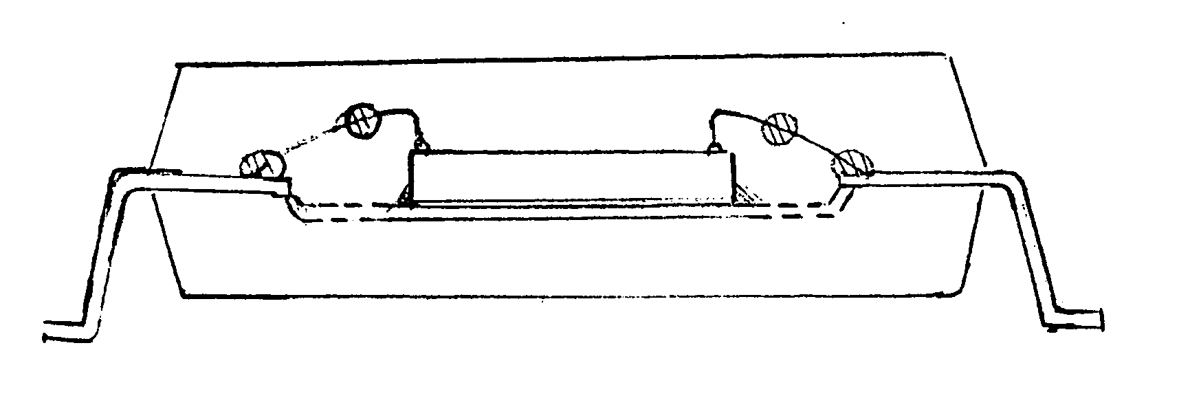
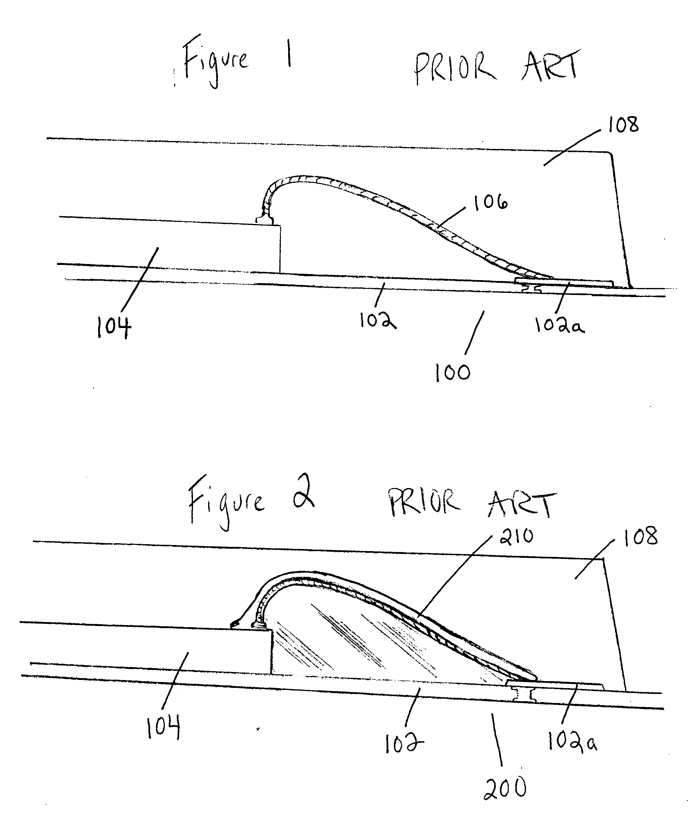
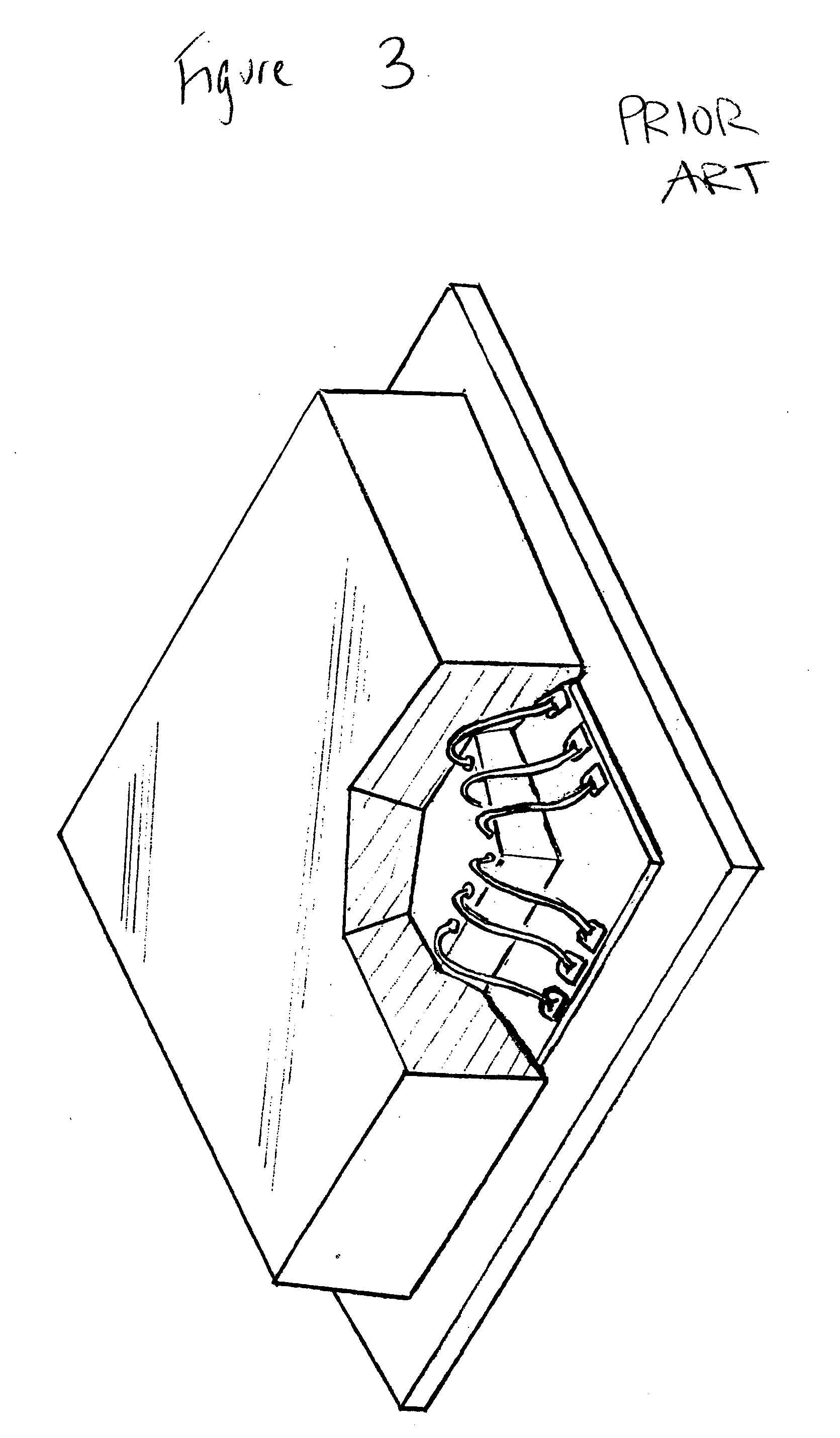
[0023] Preferred features of selected embodiments of this invention will now be described with reference to the figures. It will be appreciated that the spirit and scope of the invention is not limited to the embodiments selected for illustration. Also, it should be noted that the drawings are not rendered to any particular scale or proportion. It is contemplated that any of the configurations and materials described hereafter can be modified within the scope of this invention.

[0024] As used herein, the term semiconductor device relates to a broad category of devices including packaged semiconductor devices such as integrated circuits, memory devices, DSPs (i.e., digital signal processors), QFP (i.e., quad-flat package), PBGA (i.e., plastic ball grid array), BOC (board on chip), COB (i.e., chip on board), CABGA (chip array ball grid array), and discrete devices (i.e., non-packaged devices, may be more than one device on one board). Further, the term semiconductor element refers to ...


PUM


Abstract

A method of packaging a semiconductor device is provided. The method includes applying an insulative material across only a portion of at least two of a plurality of conductors providing interconnection between elements in the semiconductor device. The method also includes encapsulating the conductors and elements, thereby packaging the semiconductor device.

Description

FIELD OF THE INVENTION [0001] This invention relates to packaging semiconductor devices, and more particularly to a method of reducing or eliminating wire sweep and sway in packaged semiconductor devices. BACKGROUND OF THE INVENTION [0002] In the fabrication of semiconductor devices, conductors (e.g., bonding wires) are often utilized to provide interconnection between elements of the semiconductor device. For example, FIG. 1 illustrates a portion of conventional semiconductor device 100. Semiconductor device 100 includes leadframe 102 and leadframe contact(s) 102a. Semiconductor element (e.g., die) 104 is mounted on leadframe 102. Bonding wire 106 provides interconnection between semiconductor element 104 and leadframe contact 102a. Overmold 108 (i.e., a mold compound) is provided over bonding wire 106, semiconductor element 104, and leadframe contact 102a. In the configuration illustrated in FIG. 1, a number of bonding wires 106 may be included in semiconductor device 100 to provi...

Claims


Application Information

Patent Timeline
Patent Type & Authority Applications(United States)
IPC IPC(8): H01L21/44H01L21/4763H01L21/48H01L21/50H01L21/56H01L21/603H01L21/607H01L23/49H01L23/495
CPCH01L23/4952H01L23/49558H01L2924/00014H01L2924/3862H01L2924/14H01L2924/01082H01L2924/01033H01L2224/8592H01L2224/85399H01L24/48H01L24/49H01L2224/05599H01L2224/48091H01L2224/48227H01L2224/48247H01L2224/48465H01L2224/4899H01L2224/49171H01L2224/49176H01L2224/45099H01L2924/0665H01L2924/00H01L2224/73265H01L2924/181H01L2924/00012H01L2224/45015H01L2924/207H01L23/49
Inventor BATISH, RAKESHHMIEL, ANDREW F.SANDGREN, GLENNVONSEGGERN, WALTKULICKE, C. SCOTT
Owner KULICKE & SOFFA IND INC
Why Eureka
Try Eureka