Multilayer wiring board

a multi-layer wiring board and wiring board technology, applied in the direction of printed circuit non-printed electric components, sustainable manufacturing/processing, final product manufacturing, etc., can solve the problem of operation failure (disconnection) of a circuit in the multi-layer wiring board b>1/b>, and achieve the effect of low possibility of disconnection failure and high reliability

Inactive Publication Date: 2005-04-28
IBM CORP
View PDF1 Cites 22 Cited by
  • Summary
  • Abstract
  • Description
  • Claims
  • Application Information

AI Technical Summary

Benefits of technology

[0011] The multilayer wiring board of the present invention has the features that the electrode pads corresponding to the electrodes of the semiconductor chip located near the outer periphery of the semiconductor chip each have the oblong shape, the openings of the solder resist are each smaller than the oblong shape, and the center of the opening is located to be offset from the center of the oblong shape in the direction toward the center of the semiconductor chip. Therefore, in the multilayer wiring board of the present invention, thermal stresses applied to portions of the electrode pads on the board near the outer pe

Problems solved by technology

As a result, operation failure (disconnection) of a circuit in the multilayer wiring board 1 is induced.
This publication, however, discloses the technique for preventing occurrence of

Method used


Image

  • Multilayer wiring board
  • Multilayer wiring board
  • Multilayer wiring board

Examples


example

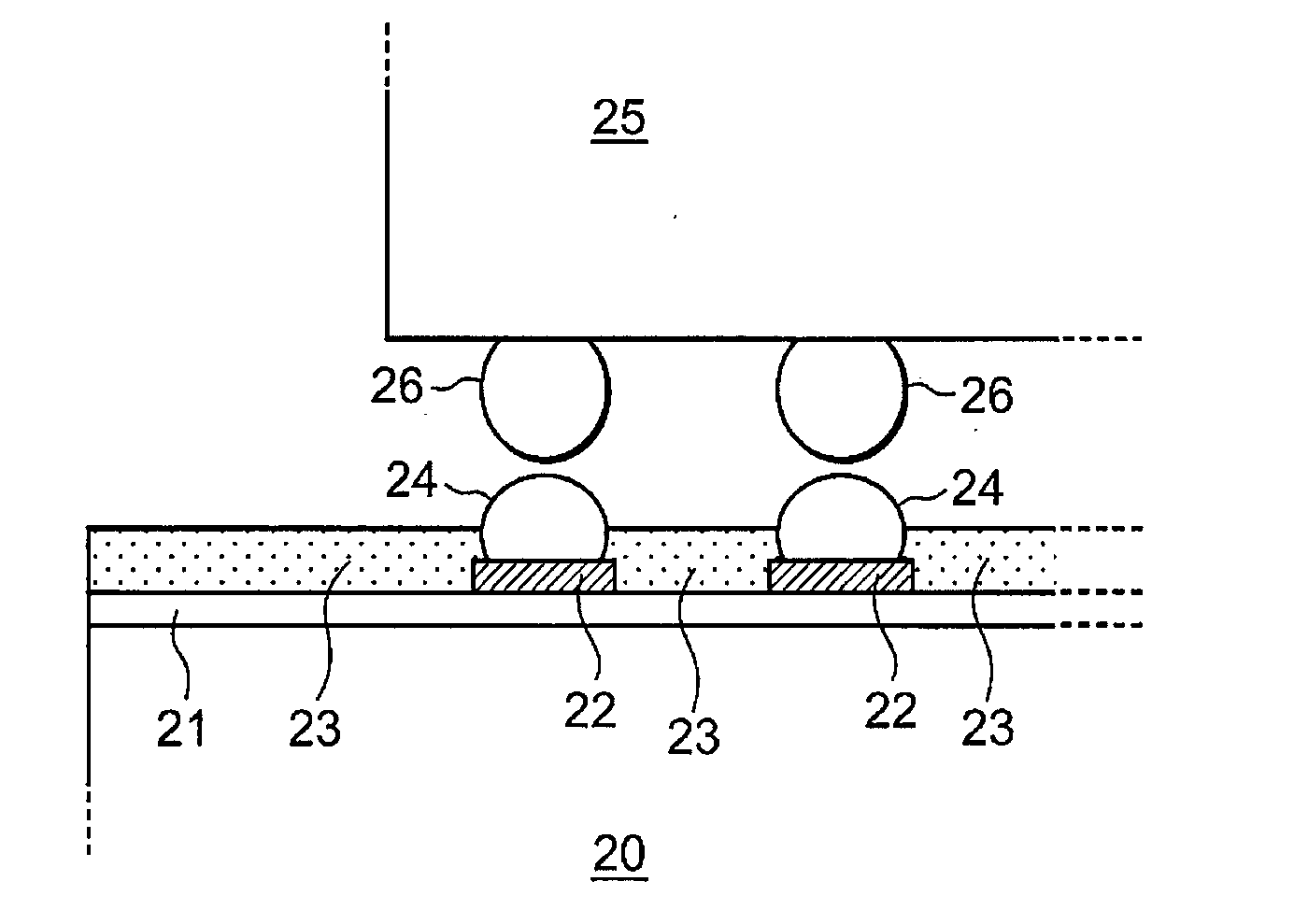
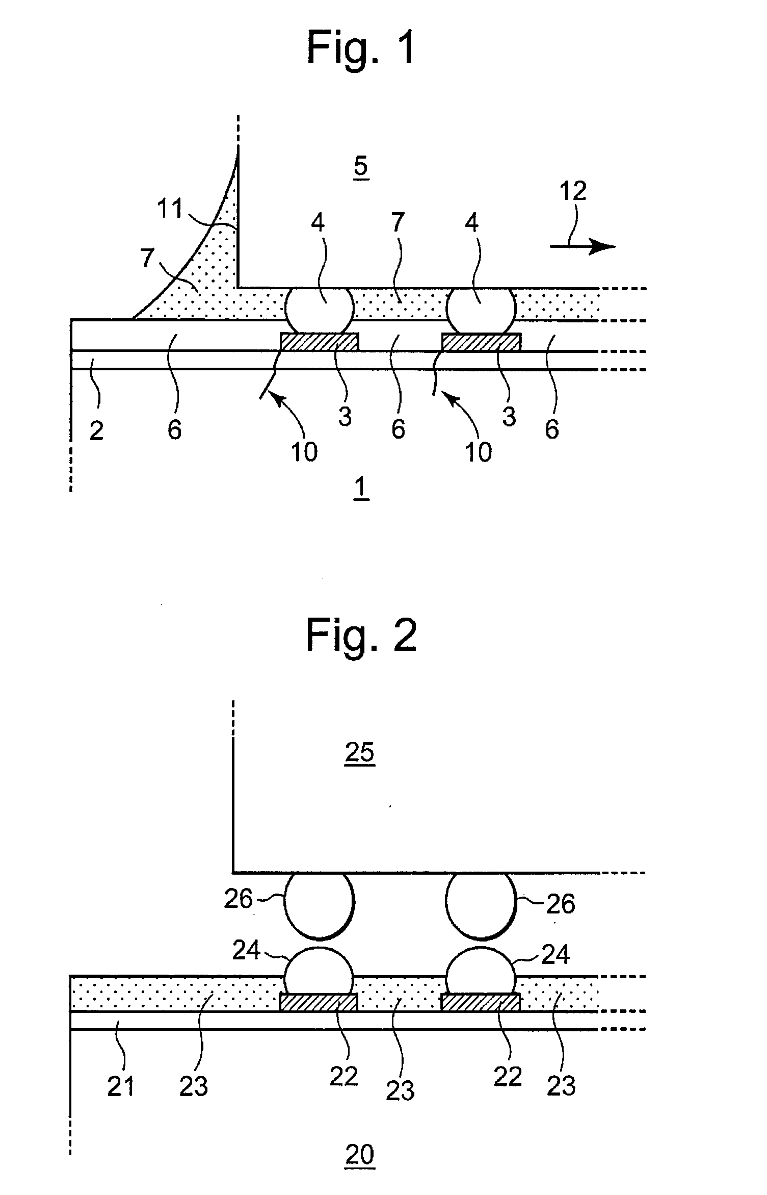
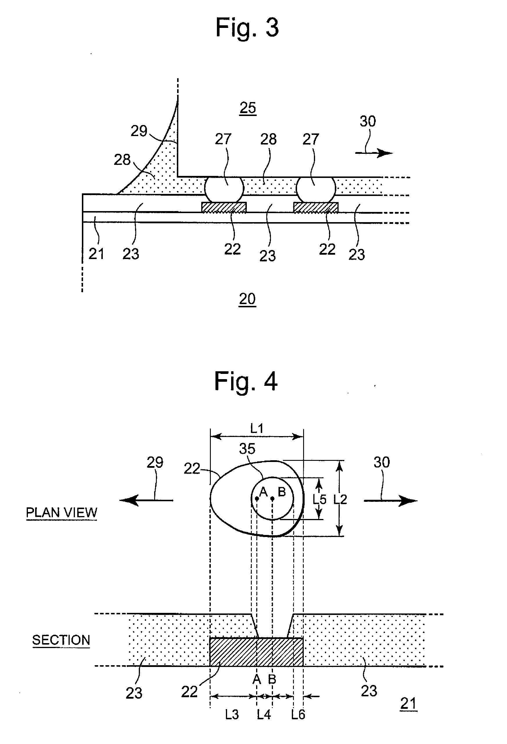
[0022] A multilayer wiring board 20 after the flip-chip bonding, having an electrode pad 22 with the shape shown in FIG. 4, was actually prepared. Dimensions (L1 to L6 in FIG. 4) of the electrode pad 22 were as follows. The unit of the dimensions is micrometer. [0023] Lateral Length of Pad 22: L1=160 to 220 [0024] Longitudinal Length of Pad 22: L2=140 to 160 [0025] Diameter of Opening 35: L5=100 [0026] Interval between Center A of Pad 22 and Center B of Opening 35: L4=10 to 40 [0027] Interval between End of Opening 35 and End of Pad 22: L6=20 to

[0028] The prepared multilayer wiring board 20 was subjected to a temperature cycle test (1250 cycles between −55° C. and 125° C.). As a result, it was confirmed that cracks corresponding to the cracks 10 shown in FIG. 1 did not occur at all.


PUM


Abstract

To prevent, in a multilayer wiring board to which a semiconductor chip is flip-chip bonded, occurrence of cracks in the board at portions adjacent to electrode pads due to a difference in thermal expansion coefficient between the semiconductor chip and the board. A multilayer wiring board (20) of the present invention has features that electrode pads (22) corresponding to electrodes of a semiconductor chip (25) located near an outer periphery (29) of the semiconductor chip each have an oblong shape, openings (35) of a solder resist (23) are each smaller than the oblong shape, and the center (B) of the opening is located to be offset from the center (A) of the oblong shape by a distance (L4) in a direction (30) toward the center of the semiconductor chip. Therefore, in the multilayer wiring board of the present invention, thermal stresses applied to portions (L3) of the electrode pads (22) on the board near the outer periphery of the semiconductor chip are relaxed. Consequently, the multilayer wiring board of the present invention can prevent occurrence of cracks in the board at portions adjacent to the electrode pads near the outer periphery of the semiconductor chip due to a difference in thermal expansion coefficient between the semiconductor chip and the board.

Description

FIELD OF THE INVENTION [0001] The present invention generally relates to a printed wiring board and, more specifically, relates to a multilayer wiring board on which a semiconductor chip is mounted by flip-chip bonding. BACKGROUND ART [0002] The flip-chip bonding is a technology of joining a semiconductor chip to electrodes on a board using solder. The flip-chip bonding is also called C4 bonding. FIG. 1 is a diagram showing the state of a semiconductor chip and a multilayer wiring board after they are flip-chip bonded together according to a conventional technique. The multilayer wiring board is a board having wiring layers and insulating layers that are stacked alternately. The multilayer wiring board is also called a multilayer board or a build-up board. Electrode pads 3 are formed on the surface of an insulating layer 2 being an uppermost layer of a multilayer wiring board 1. Each of the electrode pads 3 is located so as to correspond to an associated one of electrodes of a semic...

Claims


Application Information

Patent Timeline
IPC IPC(8): H05K3/34H01L21/60H01L23/12H01L23/498H05K1/11H05K3/46
CPCH01L23/49816H01L23/49838H01L2224/16H01L2924/01078H05K2201/10674H05K3/3436H05K3/3452H05K2201/09381H05K2201/099H05K1/111Y02P70/50
Inventor UMEMOTO, KAZUHIRO
Owner IBM CORP
Why Eureka
Try Eureka