Optical information recording medium, producing method thereof and method of recording/erasing/reproducing information
a technology of optical information and recording medium, which is applied in the direction of optical recording/reproducing/erasing methods, instruments, corona discharge, etc., can solve the problems of readout errors, phase change optical recording medium, and higher error rate of recording signals, and achieve excellent weather resistance, reproducible effect of optical information recording medium, and excellent characteristics of repetitive recording
- Summary
- Abstract
- Description
- Claims
- Application Information
AI Technical Summary
Benefits of technology
Problems solved by technology
Method used
Image
Examples
example 1
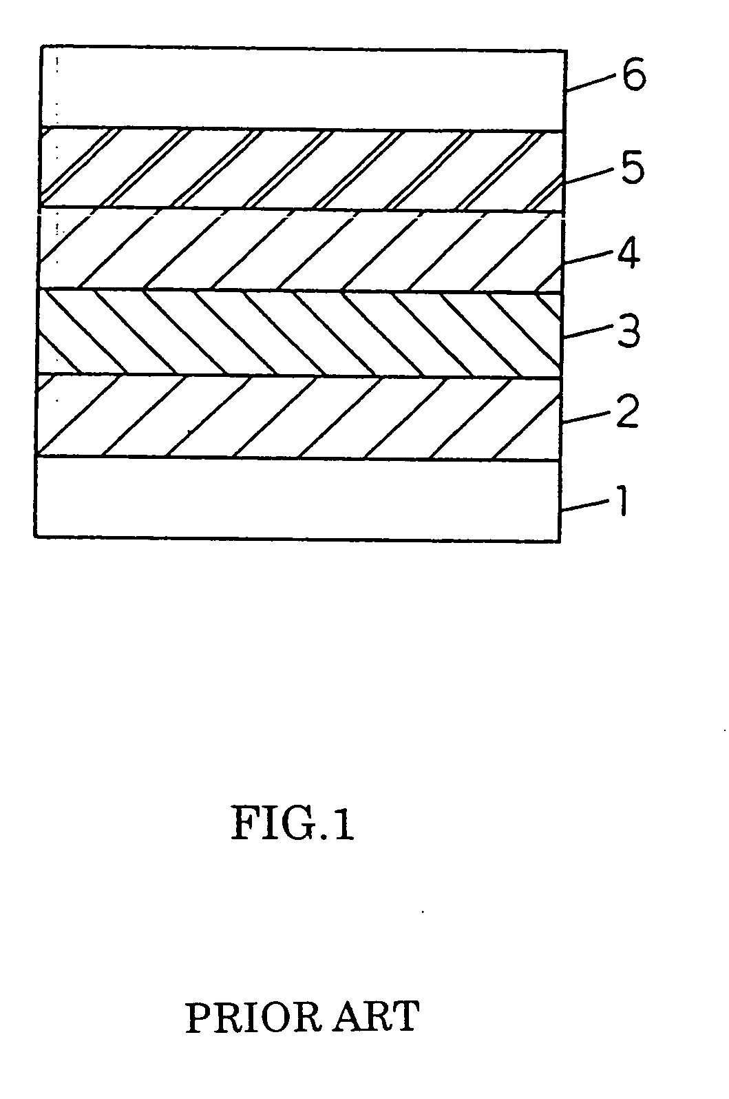
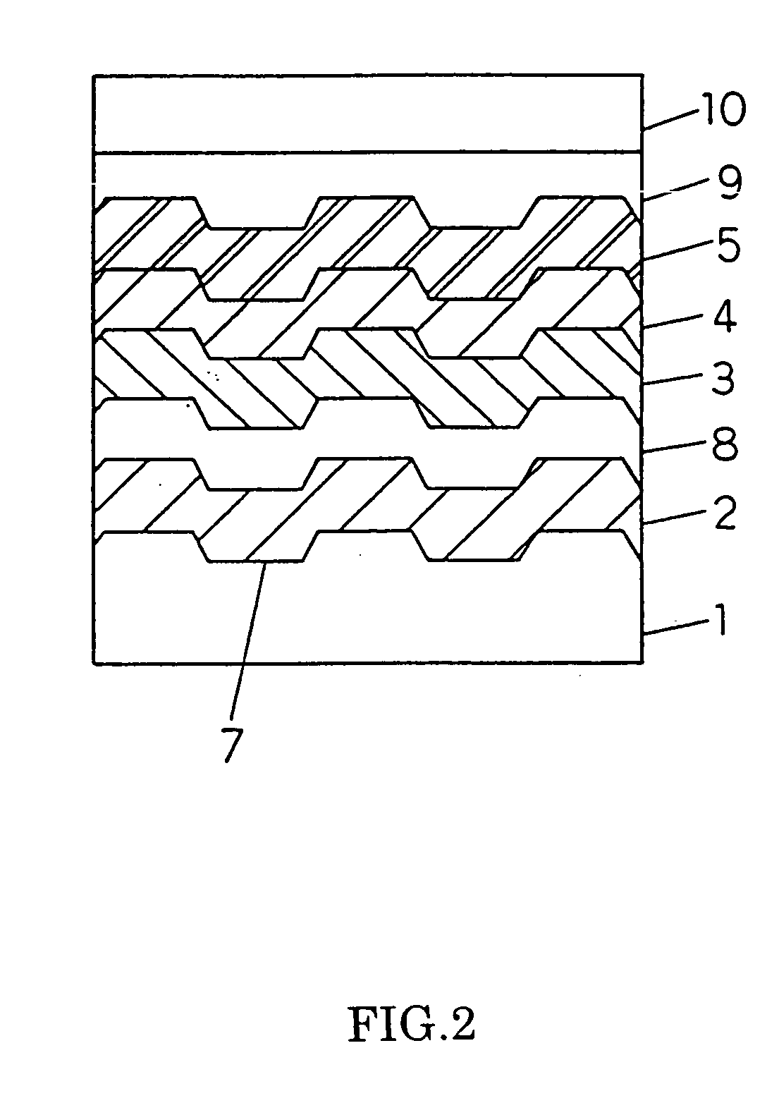
[0220] The optical disks having the layer structure shown in FIGS. 3A and 3B (a disk (1) and a disk (3) in a table 4) are made on a experimental basis. The recording layer 3 comprises a phase change material whose main component is a Ge2Sb2.3Te5 alloy, and the dielectric protective layers 2 and 4 comprises a ZnS—SiO2 film. When the film is formed, the gas is supplied in such a manner that each total pressure of the Ar gas becomes 1.0 mTorr and 0.5 mTorr, respectively, and each of the powers DC1.27 W / cm2 and RF6.37 W / cm2 is introduced into the negative electrode 55, respectively. Furthermore, when the reflecting layer (AlCr) 5 is formed, the Ar gas is supplied in such a manner that the total pressure becomes 3.0 mTorr, thereby the power DC 4.45 W / cm2 is introduced.
[0221] In the disk (1), after the dielectric protective layer is formed, sequentially, the barrier layer 8 is formed. In the disk (3), after the recording layer 3 is formed, sequentially, the barrier layer 8 is formed. In ...
example 2
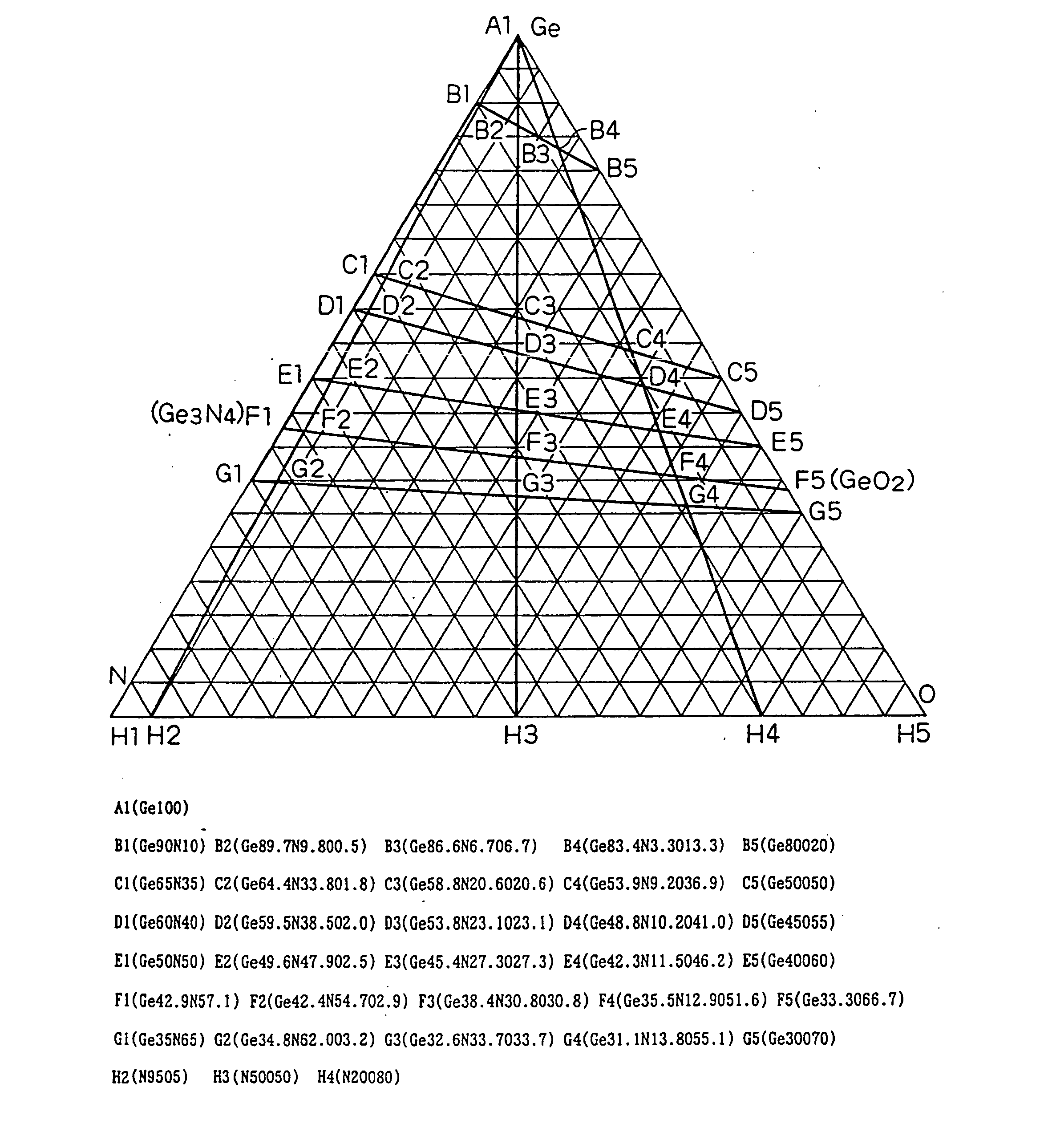
[0225] All the protective layers at the substrate side of the disk (1) in Table 4 in the example 1 are changed to the Ge—N layer or the Ge—N—O layer, thereby a disk (5) is formed (accordingly, the Ge—N protective layer or the Ge—N—O protective layer whose thickness is 91 nm is formed at the substrate side of the recording layer). Furthermore, all the protective layers at the reflecting layer side of the disk (3) in Table 4 are changed to the Ge—N layer or the Ge—N—O layer, thereby a disk (6) is formed (accordingly, the Ge—N protective layer or the Ge—N—O protective layer whose thickness is 25.2 nm is formed at the reflecting layer side of the recording layer). The repeating characteristic of disks (5) and (6) is examined by the same method as the example 1. Both of them can similarly obtain the result ⊚. That is, the Ge—N layer or the Ge—N—O layer can be formed in such a manner that the Ge—N layer or the Ge—N—O layer can obtain a thickness necessary for the protective layer. Further...
example 3
[0226] Next, the recording layer 3 comprises a phase change material whose main component is a Ge2Sb2.3Te5 alloy, when the barrier layer 8 is formed, Sb is used as the target, and the mixture of Ar and nitrogen is used as the sputter gas. On the above condition, the films comprising the structure shown in FIGS. 3A and 3B are formed (a disk (2), a disk (4)). In this case, the film thickness of each layer is same as the thickness in the above case that Ge is used as the target. The spatter gas pressure of the barrier layer 8 is 20 mTorr, and the partial pressure ratio of Ar to nitrogen in the sputter gas is 3 to 1. In this case, the result of the repeating characteristic is shown in disk numbers (2) and (4) in Table 4.
[0227] According to Table 4, compared to the case that Ge is used as the target so that the film is formed, although the number of repeatable times is inferior, better repeating characteristic can be obtained than the comparative example.
TABLE 4Result 3 of comparing t...
PUM
 Abstract
Description
Claims
Application Information
 - R&D
- Intellectual Property
- Life Sciences
- Materials
- Tech Scout
- Unparalleled Data Quality
- Higher Quality Content
- 60% Fewer Hallucinations
Browse by: Latest US Patents, China's latest patents, Technical Efficacy Thesaurus, Application Domain, Technology Topic, Popular Technical Reports.
© 2025 PatSnap. All rights reserved.Legal|Privacy policy|Modern Slavery Act Transparency Statement|Sitemap|About US| Contact US: help@patsnap.com


