Electro-optical device, method of manufacturing the same, and electronic apparatus

a technology of electro-optical devices and electronic devices, applied in the direction of optical waveguides, light guides, waveguides, etc., can solve the problems of deterioration of the reliability of the electro-optical devi

Active Publication Date: 2005-06-02
SEIKO EPSON CORP
View PDF3 Cites 74 Cited by
  • Summary
  • Abstract
  • Description
  • Claims
  • Application Information

AI Technical Summary

Benefits of technology

[0020] In the present invention, when the electro-optical device further comprises a light source for emitting light toward the first member, the first member is made of a transmissive material, and is used as a light guide plate for transmitting light emitted from the light source toward the electro-optical device substrate through the curved surface, which is a light exit surface. When the electro-optical device is a transmissive or transflective liquid crystal device, a backlight unit is provide on the rear side of the liquid crystal panel. In this case, when the liquid crystal panel is curved, light emitted from the backlight unit is non-uniformly incident on the liquid crystal panel. As a result, a bright region and a dark region are formed on the image display surface of the electro-optical device. However, according to the present invention, since the first member is used as the light guide plate, uniform light can be emitted toward the entire surface of the electro-optical device substrate through the first member, which is the light guide plate. Therefore, it is possible to display a high-quality image without the bright region and the dark region on the image display surface of the electro-optical device.

Problems solved by technology

However, when a polymer film is used as an electro-optical device substrate, the reliability of an electro-optical device deteriorates because the polymer film has low weather resistance ard heat resistance.

Method used


Image

  • Electro-optical device, method of manufacturing the same, and electronic apparatus
  • Electro-optical device, method of manufacturing the same, and electronic apparatus
  • Electro-optical device, method of manufacturing the same, and electronic apparatus

Examples


first embodiment

(Basic Structure of Electro-optical Device)

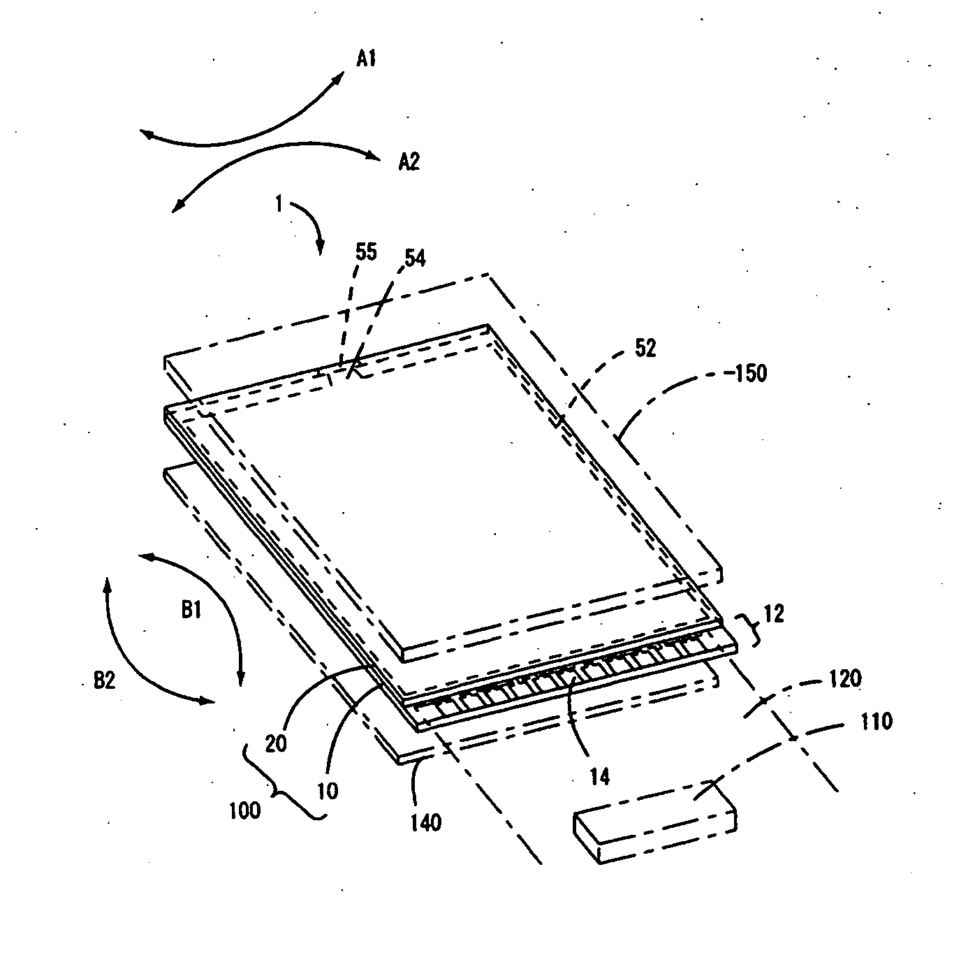
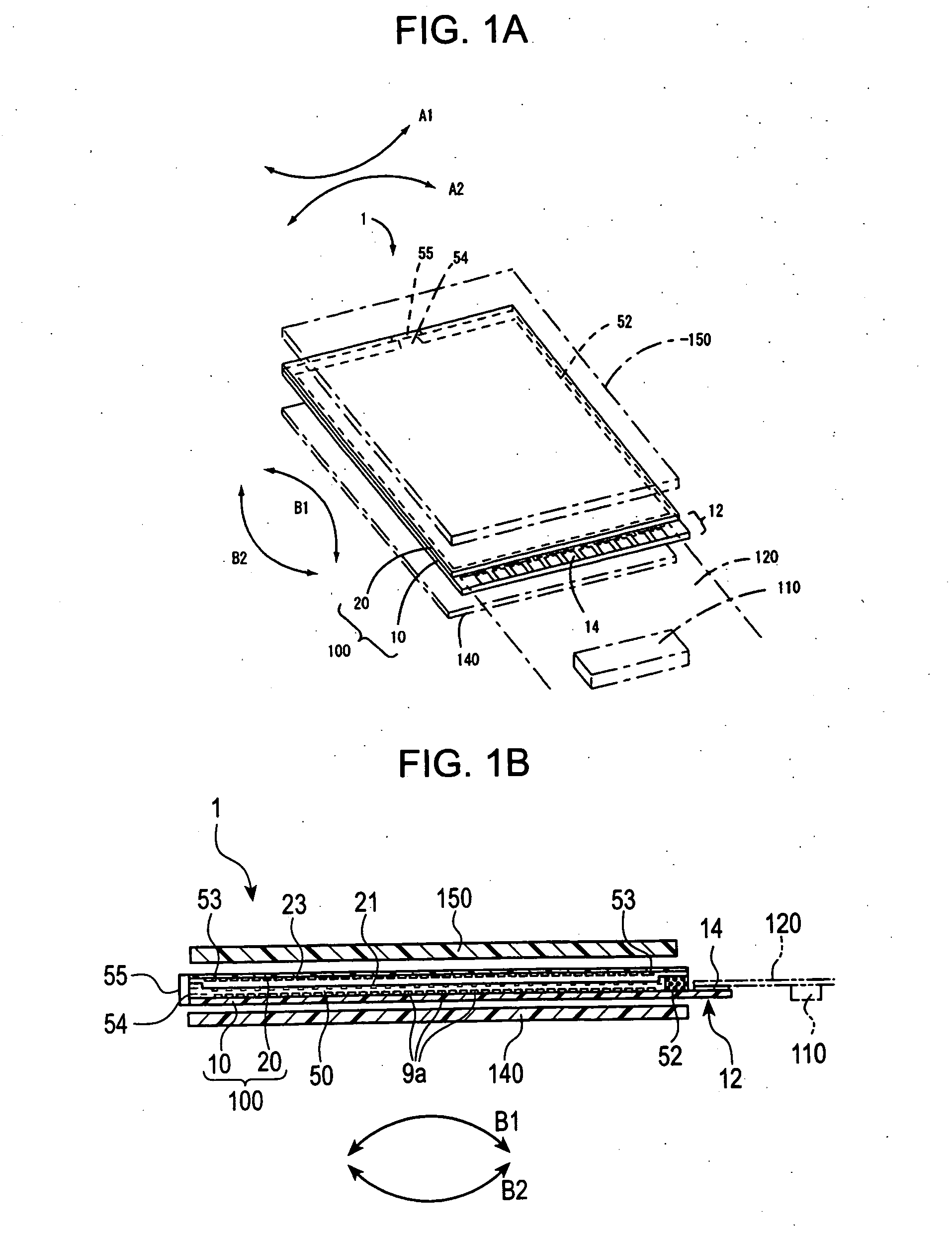
[0041]FIG. 1(A) is a view illustrating the structure of an electro-optical device according to the present invention as seen from the counter substrate side, and FIG. 1(B) is a cross-sectional view thereof. FIG. 2 is an equivalent circuit diagram for various elements and wiring lines of a plurality of pixels that is arranged in a matrix in an image display region of the electro-optical device. In the drawings used for explaining the present invention, since each layer or each member is scaled to be recognizable in the drawings, the reduced scale of each layer or each member differs from the actual scale thereof.

[0042] In FIGS. 1(A) and 1(B), an electro-optical device 1 according to the first embodiment comprises a transmissive or transflective active matrix liquid crystal panel 100. In the liquid crystal panel 100, liquid crystal 50, which is an electro-optical material, is held between a TFT array substrate 10 (an electro-optical device...

second embodiment

[0062]FIG. 5 is a cross-sectional view illustrating the structure of an electro-optical device according to the second embodiment of the present invention. In the present embodiment and other embodiments to be described later, since their basic structures are the same as that in the first embodiment, components having the same function are represented by the same reference numeral, and thus a description thereof will be omitted.

[0063] In FIG. 5, the structure of an electro-optical device 1 according to the present embodiment is equal to that in the first embodiment, except that the side of the base 210 is used as a display surface. In the electro-optical device 1 having such a structure, when the liquid crystal panel 100 is a transmissive type, light (which is indicated by arrow L2) emitted from a backlight unit is optically modulated in the liquid crystal panel 100, and then exits therefrom as display light (which is indicated by arrow L10). On the other side, when the liquid crys...

third embodiment

[0064] In the first embodiment, the spacers 260 and 270 are respectively arranged between the liquid crystal panel 100 and the first and second polarizing plates 140 and 150. However, in the present embodiment, as described below, sheets having unevenness thereon are used instead of the spacers 260 and 270 in order to prevent the generation of Newton's ring.

[0065]FIG. 6 is a cross-sectional view illustrating the structure of an electro-optical device according to the third embodiment of the present invention.

[0066] As shown in FIG. 6, in an electro-optical device 1 of the present embodiment, a base 210 having a curved surface 220, a first polarizing plate 140, a liquid crystal panel 100, ard a second polarizing plate 150 having an area larger than that of the liquid crystal panel 100 are superposed in this order. In addition, a first sheet 160 having unevenness is arranged between the first polarizing plate 140 and the liquid crystal panel 100, and a second sheet 170 having uneven...


PUM

PropertyMeasurementUnit
thicknessaaaaaaaaaa
thicknessaaaaaaaaaa
thicknessaaaaaaaaaa

Abstract

A method of manufacturing an electro-optical device having a curved display surface with high reliability is provided. A liquid crystal panel 100 comprising a TFT array substrate 10 and a counter substrate 20, each composed of a glass substrate or a quartz substrate, is thinned down to, for example, a thickness of 25 μm by a polishing process or an etching process. Subsequently, a first polarizing plate 140, first spacers 260, the liquid crystal panel 100, second spacers 270, and a second polarizing plate 150 are superposed on a base 210 having a curved surface 220 in this order, and then the outer circumference of the second polarizing plate 150 is pressed against the base 210 while curving the second polarizing plate 150 along the curved surface 220 of the base 210. Then, in order to maintain such a curved state, the second polarizing plate 150 is fixed to the base 210 by a double-faced tape 280.

Description

BACKGROUND OF THE INVENTION [0001] 1. Field of Invention [0002] The present invention relates to an electro-optical device in which an electro-optical material is held in a substrate, an electronic apparatus using the same, and a method of manufacturing the electro-optical device. [0003] 2. Description of Related Art [0004] In general, in electro-optical devices, such as liquid crystal devices and organic electro-luminescent display device, an electro-optical material is held by an electro-optical device substrate, and various images are displayed on a substantially central region of the substrate, which is an image display region. [0005] In recent years, the development of the new type of display device having an electro-optical device in which its display surface is curved has been required. Complying with such requirements, it has been suggested that a flexible polymer film is used as an electro-optical device substrate such that the electro-optical device substrate can be curved...

Claims


Application Information

Patent Timeline
Patent Type & Authority Applications(United States)
IPC IPC(8): G02B26/00G02F1/00G02F1/035G02F1/1333G09G3/12G09G3/18
CPCG02F1/1333Y10S385/901G02F2202/09G02F1/133305
Inventor IDE, KATSUYA
Owner SEIKO EPSON CORP
Why Eureka
Try Eureka