[0011] A further object of the present invention is to provide a method of fabricating a plurality of capacitors having sufficient
capacitance by increasing the height of lower plates, while preventing leaning of the lower plates during the fabrication process.
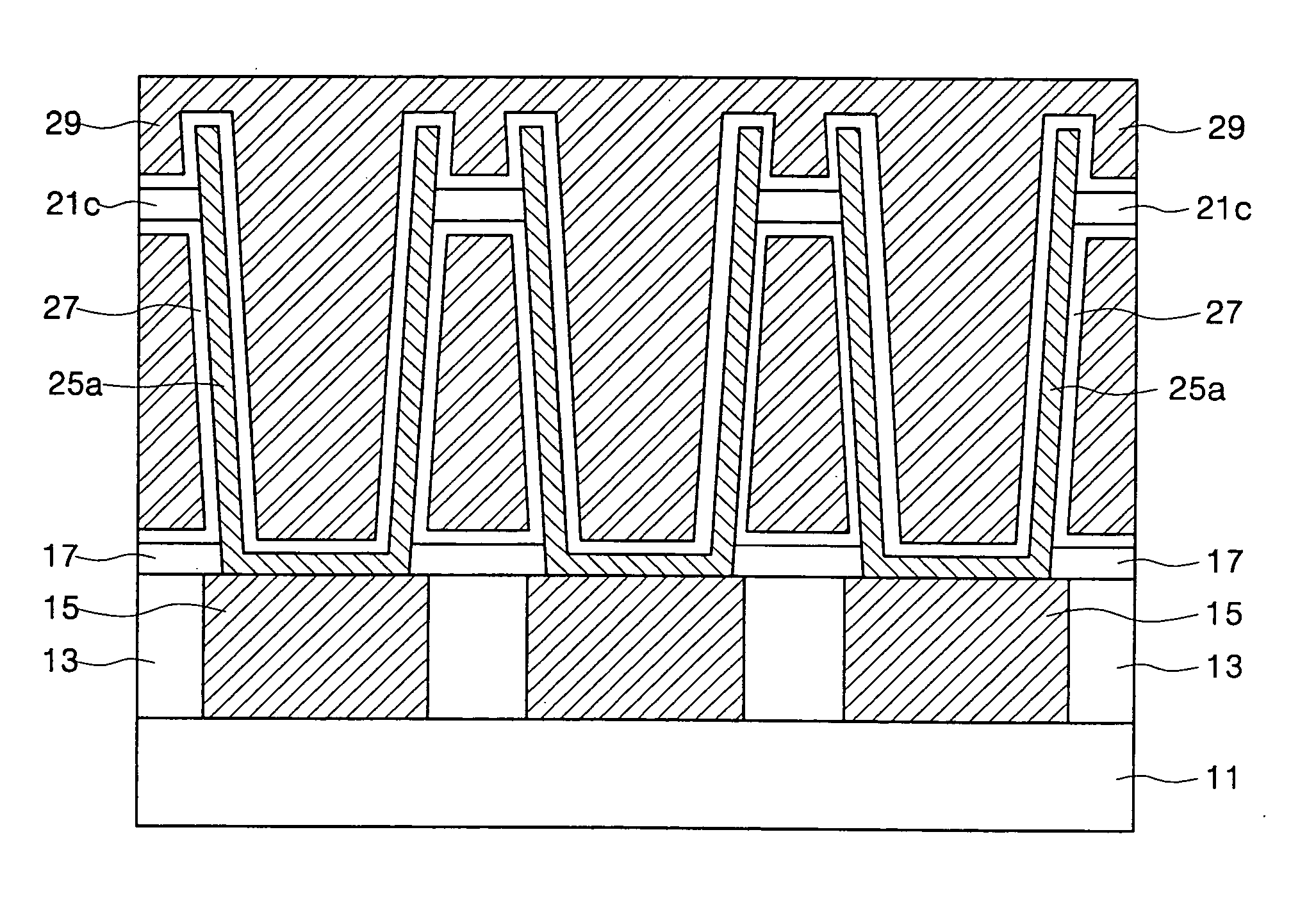
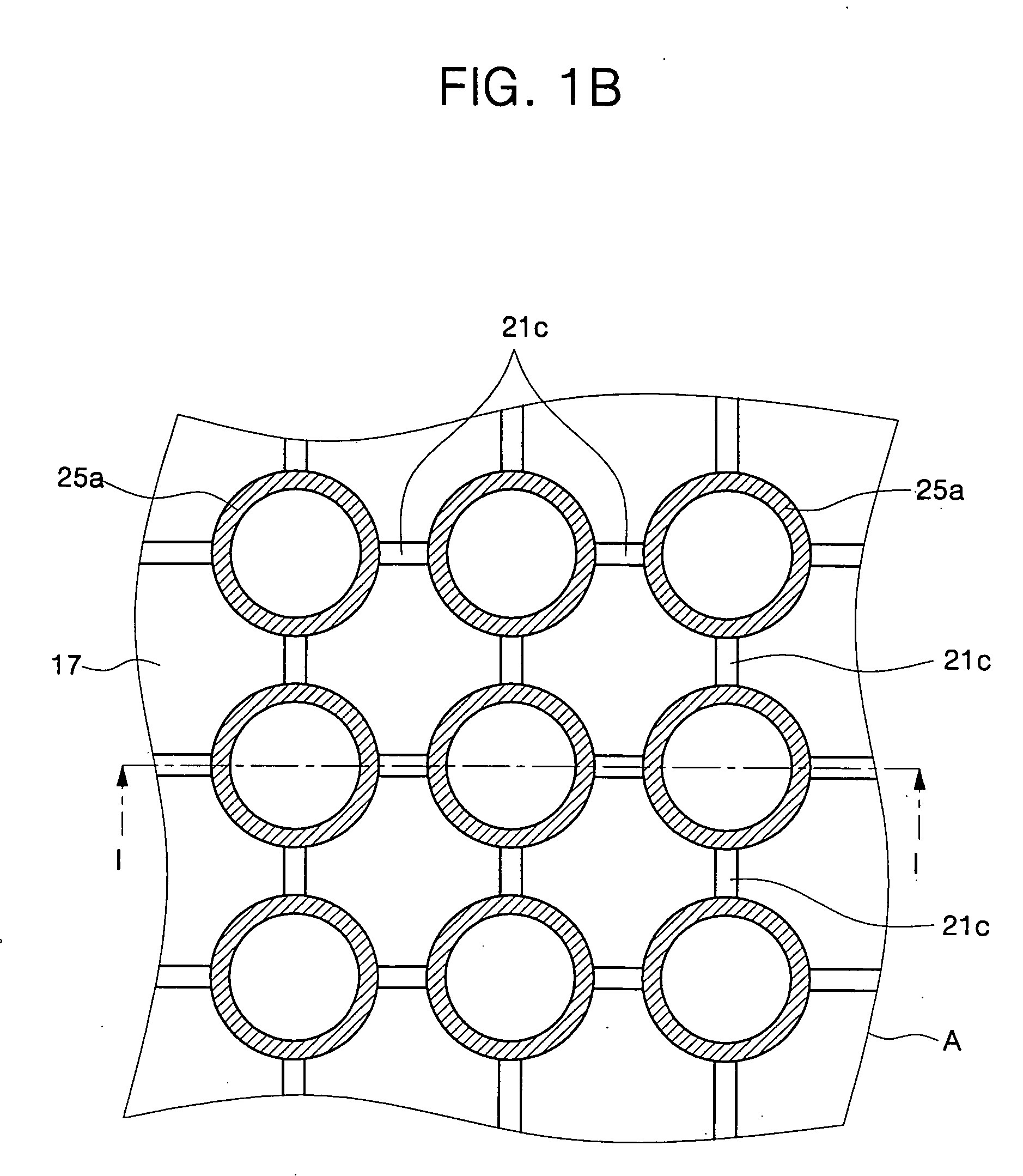
[0012] In accordance with an. exemplary embodiment, the present invention provides a plurality of capacitors employing holding layer patterns. The plurality of capacitors include a plurality of cylinder-shaped lower plates repeatedly aligned on a same plane in two dimensions. Holding layer patterns are located between uppermost portions and lowermost portions of the plurality of lower plates, and connect the adjacent side walls of the plurality of lower plates. An upper plate fills the spaces inside the plurality of lower plates and the spaces between the side walls thereof. A
capacitor dielectric layer is interposed between the plurality of lower plates and the upper plate, and insulates the lower plates and the upper plate. As such, the holding layer patterns are located between the side walls of the lower plates to support the lower plates. As a result, the structure serves to avoid leaning of the lower plates.
[0018] In accordance with an exemplary embodiment, the present invention provides a
semiconductor device having a plurality of capacitors employing holding layer patterns. The
semiconductor device includes a semiconductor substrate. A plurality of cylinder-shaped lower plates are aligned repeatedly over the semiconductor substrate in two dimensions. Holding layer patterns are located between uppermost portions and lowermost portions of the plurality of lower plates, and connect the adjacent side walls of the plurality of lower plates. An upper plate fills the spaces inside the plurality of lower plates and the spaces between the side walls thereof. A capacitor
dielectric layer is interposed between the plurality of lower plates and the upper plate, and insulates the lower plates and the upper plate.
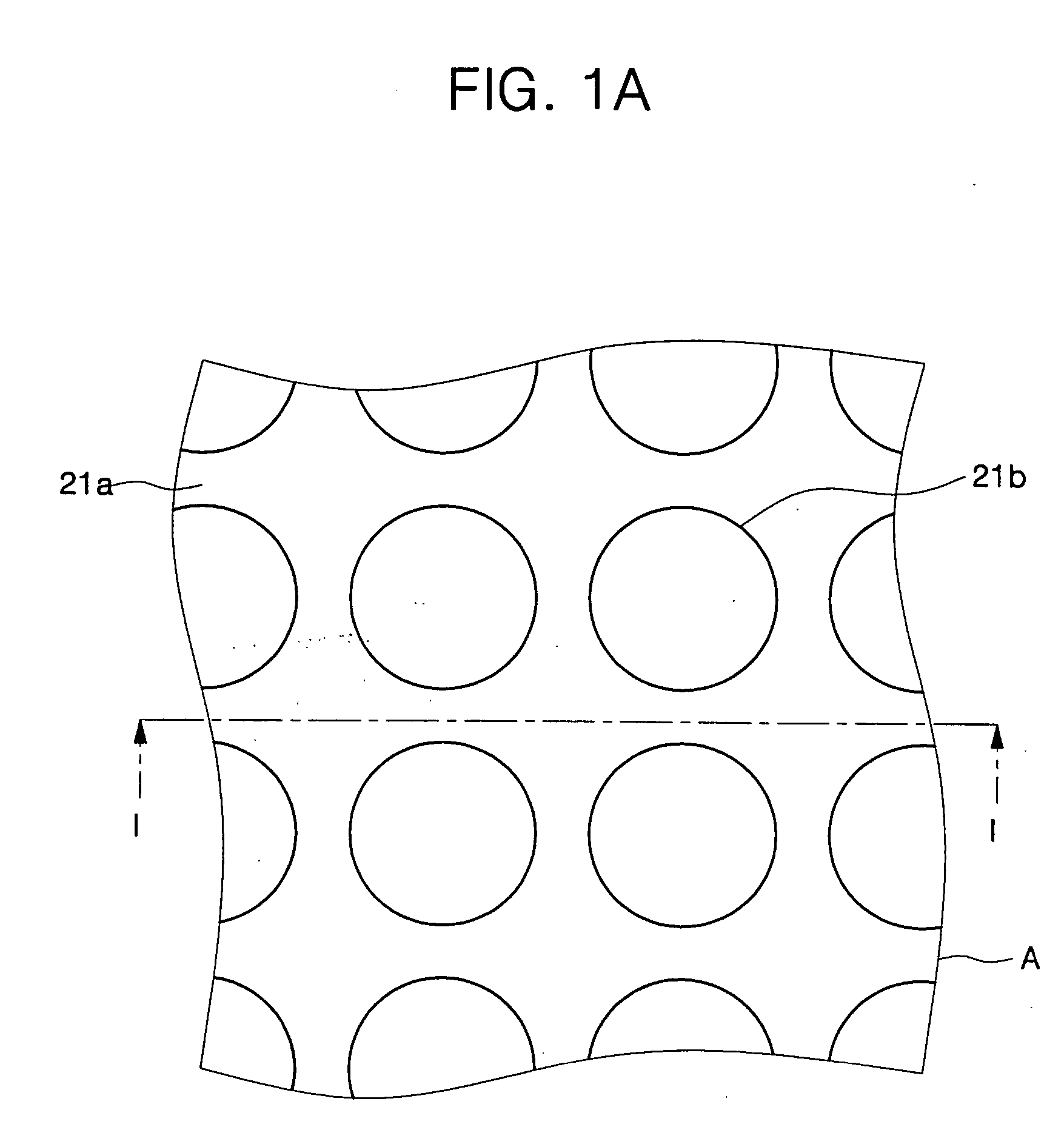
[0020] In accordance with a further exemplary embodiment, the present invention provides a method of fabricating a plurality of capacitors employing holding layer patterns. The method includes preparing a semiconductor substrate having a lower insulating layer. A plurality of storage contact plugs repeatedly aligned in two dimensions are formed inside the lower insulating layer. An etch
barrier layer and a lower sacrificial
oxide layer are sequentially formed on the semiconductor substrate having the storage contact plugs. A holding layer having openings exposing the lower sacrificial
oxide layer is formed on the lower sacrificial
oxide layer. Herein, the centers of the respective openings are located above portions of the lower insulating layer that are surrounded by the storage contact plugs. An upper sacrificial oxide layer is formed over the semiconductor substrate having the holding layer with the openings. The upper sacrificial oxide layer, the holding layer, the lower sacrificial oxide layer, and the etch
barrier layer are sequentially patterned using
photolithography and etch processes, to form capacitor holes exposing the storage contact plugs and holding layer patterns. The holding layer patterns are exposed inside the capacitor holes. Then, lower plates covering the inner walls of the capacitor holes are formed, and the upper sacrificial oxide layer and the lower sacrificial oxide layer between the lower plates are sequentially removed. As the holding layer patterns support the lower plates, even though the upper sacrificial oxide layer and the lower sacrificial oxide layer between the lower plates are removed, falling-down of the lower plates can be avoided.
[0024] In accordance with another exemplary embodiment, the present invention provides a method of fabricating a plurality of capacitors employing holding layer patterns. The method includes preparing a semiconductor substrate having a lower insulating layer. A plurality of storage contact plugs repeatedly aligned in two dimensions are formed inside the lower insulating layer. An etch
barrier layer and a lower sacrificial oxide layer are sequentially formed on the semiconductor substrate having the storage contact plugs, and the lower sacrificial oxide layer is partially etched to form grooves repeatedly aligned in two dimensions. Herein, the centers of the respective grooves are located above portions of the lower insulating layer that are surrounded by the storage contact plugs. Then, spacers covering the inner walls of the grooves are formed. An upper sacrificial oxide layer is formed on the semiconductor substrate having the spacers. The upper sacrificial oxide layer, the spacers, the lower sacrificial oxide layer, and the etch barrier layer are sequentially patterned using
photolithography and etch processes, to form capacitor holes exposing the storage contact plugs and holding layer patterns. Herein, the holding layer patterns are exposed inside the capacitor holes. Then, lower plates covering the inner walls of the capacitor holes are formed, and the upper sacrificial oxide layer and the lower sacrificial oxide layer between the lower plates are sequentially removed. As the holding layer patterns are formed of spacers having a wide lower side and a narrow upper side, it is easy to form a following capacitor
dielectric layer and an upper plate between the lower plates. Thus, the height of the holding layer patterns can be increased.


