Testing of integrated circuits using boundary scan

a technology for integrated circuits and boundary scans, applied in digital circuit testing, electronic circuit testing, measurement devices, etc., can solve the problems of difficult testing of difficult to write test software for jtag testing, and difficult to test the connection between the bga chip and its board. achieve the effect of facilitating the creation of test scripts

Inactive Publication Date: 2005-05-05
MIDAS YELLOW
View PDF3 Cites 30 Cited by
  • Summary
  • Abstract
  • Description
  • Claims
  • Application Information

AI Technical Summary

Benefits of technology

[0015] The invention facilitates the creation of test scripts for testing of integrated circuits using boundary-scan architecture, and in particular the development of test scripts that ar...

Problems solved by technology

It is a problem with BGA circuits that the pins are not individually accessible by test equipment, because they are buried underneath the IC package.
An IC itself can be tested using a “bed of nails” test jig, but it is a problem that, in situ, the connection between the BGA chip and its board is difficult to test, because it is inaccessible.
Writing test software to perform JTAG testing is extremely complex and labour-intensive.
Testing is further complicated by the fact that each pin can take one of three states: a high state, a low state, or an input state.
Common faults that need to be identified include connection breaks (for example whether the solder has failed to connect a pin to its pad), connection shorts (e.g. where solder has spi...

Method used


Image

  • Testing of integrated circuits using boundary scan
  • Testing of integrated circuits using boundary scan
  • Testing of integrated circuits using boundary scan

Examples


Embodiment Construction

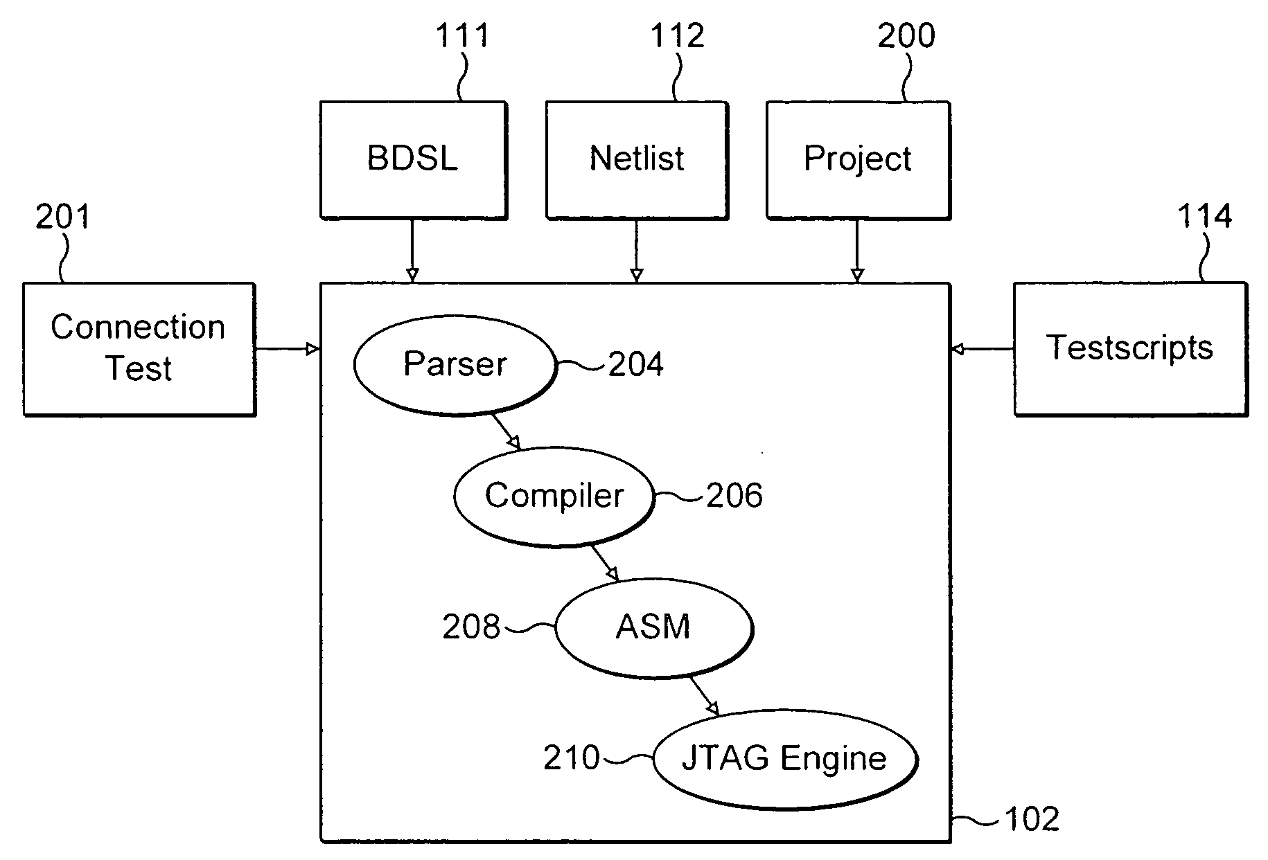
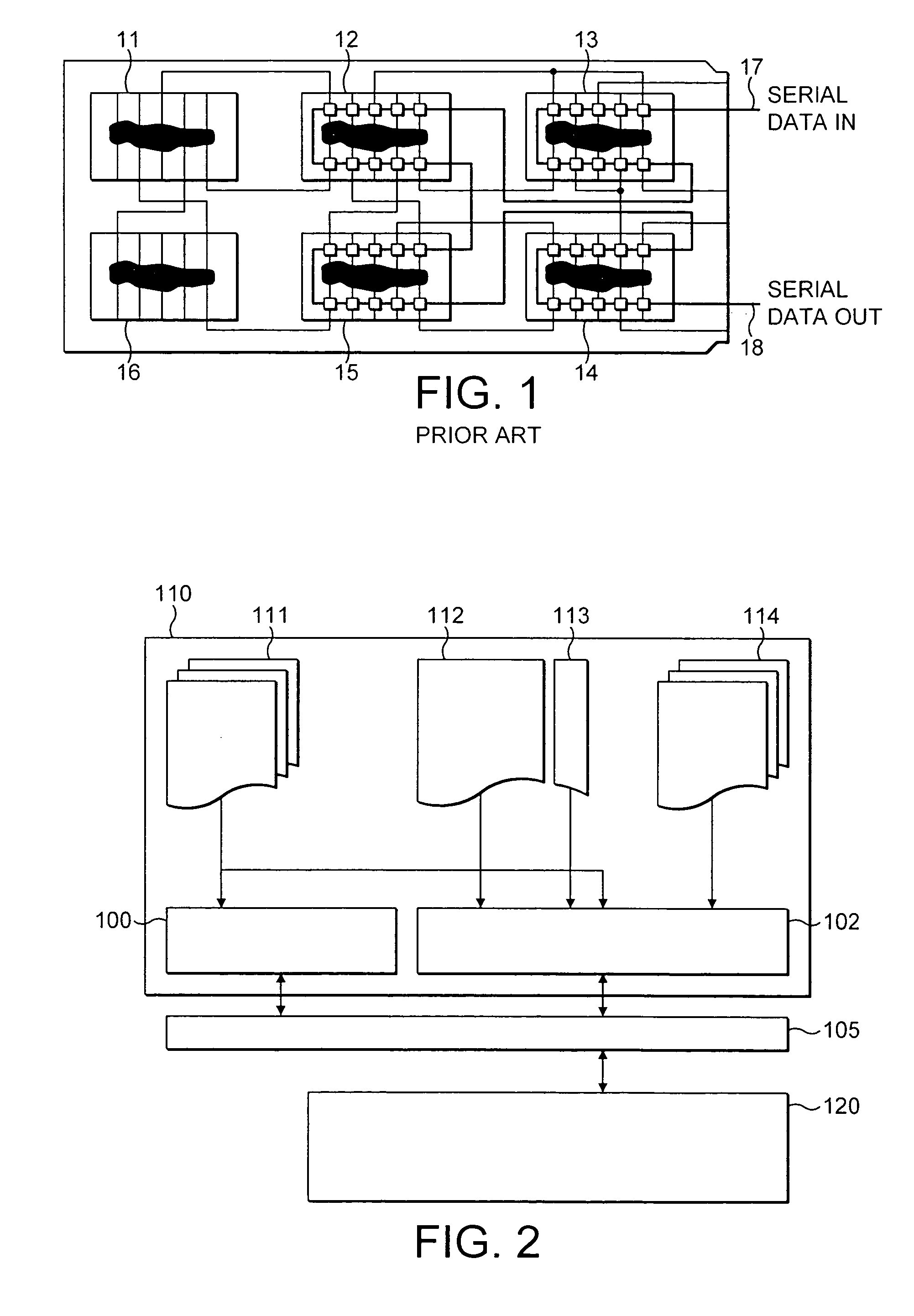
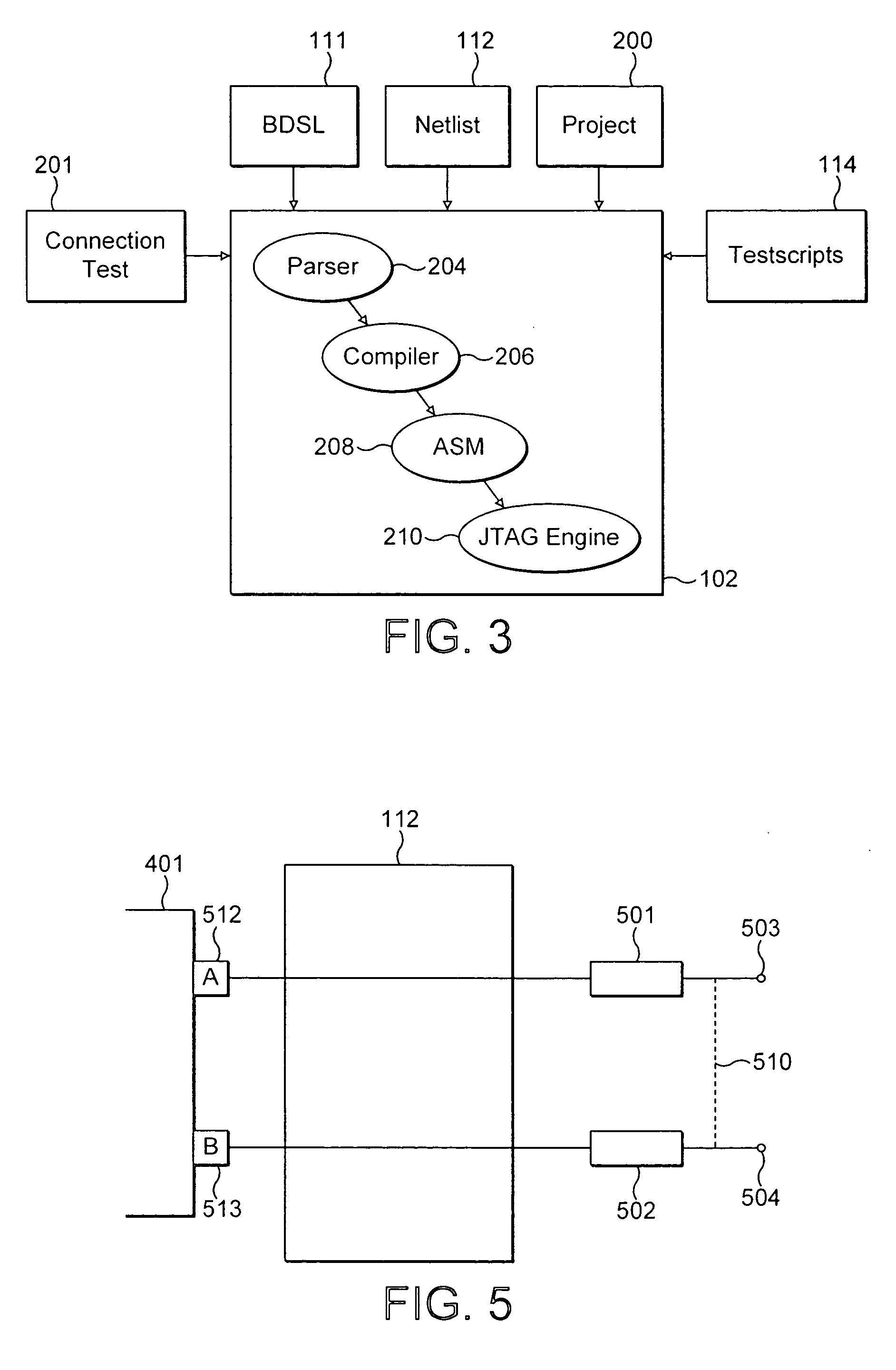
[0020] Referring to FIG. 2, the equipment of the present invention comprises analyser software 100 and test software 102, which are run on a computer 110 that is connected via an adapter 112 to a board 120 that is to be tested. The test software 102 is stored in a high level language as described below. Loaded into the computer 100 are boundary-scan description language (BSDL) files 111, a netlist 112 and a set of test scripts 114. Beside the netlist 112 is shown a connections list 113.

[0021] Each BSDL file 111 is supplied by the manufacturer of a particular IC and defines, for that IC the manner in which JTAG is implemented. BSDL files contain the following elements: [0022] Entity Description: Statements naming the device or a section of its functionality. [0023] Generic Parameter: A value such as a package type. The value may come from outside the current entity. [0024] Port Description: Describes the nature of the pins on the device (input, output, bidirectional, linkage). [0025...


PUM


Abstract

Circuit testing equipment comprising a computer (110) having stored thereon a boundary scan description language (BSDL) file (111), a netlist (112) and a connections list (113). An adapter (105) connects the computer to a boundary scan bus of a circuit (120) to be tested. The computer is arranged to parse and compile the BSDL file, the netlist and the connections list to generate a data structure which, when combined with a test script (114), permits execution of the test script from the computer through the boundary scan bus. The test script can be IC-specific such that it is valid for a particular IC independent of the circuit in which the IC is located.

Description

FIELD OF THE INVENTION [0001] This invention relates to methods and equipment for testing of integrated circuits using boundary scan capability and architecture. [0002] As integrated circuits (ICs) have become smaller and smaller, the ball grid array (BGA) format of pin connection has become popular. BGA circuits have an array of pins on the underside of the IC package and a corresponding array of pads on the surface of a multi-layer printed circuit board (PCB). Between each pin on the IC package and each corresponding pad on the board, there is a ball of solder which, during reflow processing, solders the pin to its corresponding pad. The arrangement has advantages over packages that have their pins around the outside edge of the package, because these latter packages cannot be reduced in size below the minimum separation possible for the pins that extend around the outside edge of the package. By contrast, BGA pins with the same pin separation distance can occupy a smaller package...

Claims


Application Information

Patent Timeline
IPC IPC(8): G01R31/28G01R31/3185G01R31/319
CPCG01R31/31917G01R31/318547
Inventor PLUNKETT, DOMINIC
Owner MIDAS YELLOW
Why Eureka
Try Eureka