Processing apparatus using laser beam

a processing apparatus and laser beam technology, applied in the direction of laser beam welding apparatus, stone-like material working apparatus, manufacturing tools, etc., can solve the problem of insufficient satisfactory processing apparatus, inability to generate the thickness of the necessary thickness to break the wafer sufficiently precisely, and inability to achieve the desired deterioration

Active Publication Date: 2005-05-12
DISCO CORP
View PDF30 Cites 103 Cited by
  • Summary
  • Abstract
  • Description
  • Claims
  • Application Information

AI Technical Summary

Benefits of technology

[0006] It is a principal object of the present invention, therefore, to provide a novel and improved processing apparatus using a laser beam, the processing apparatus being capable of generating deterioration, as desired, on at least two focus points displaced in the thickness direction of a workpiece, while ingeniously avoiding a situation where deterioration of one of the two focus points inhibits application of a pulsed laser beam to the other focus point, thereby generating a deterioration region of a required thickness in the workpiece.
[0007] We, the inventors, diligently conducted studies and experiments, and have found the following facts: A pulsed laser beam is focused, with some time difference provided, to at least two focus points displaced in the optical axis direction of the pulsed laser beam, accordingly, displaced in the thickness direction of a workpiece. As a result, a situation where deterioration at one of the focus points inhibits application of the pulsed laser beam to the other focus point can be avoided. Thus, the aforementioned principal object can be attained.
[0010] In the processing apparatus using a laser beam according to the present invention, a time difference is caused to exist in the focusing of the pulsed laser beam at each of at least two focus points. Hence, a situation where deterioration generated at one of the focus points inhibits application of the pulsed laser beam to the other focus point is avoided. Consequently, deterioration, as desired, can be generated on at least two focus points.

Problems solved by technology

If the thickness of the wafer is relatively large, therefore, it takes a relatively long time to generate the deterioration region of a necessary thickness to break the wafer sufficiently precisely.
However, the processing apparatus is still not sufficiently satisfactory, but poses the following problems to be solved: Deterioration at one of the two focus points, more specifically, the focus point at a shorter distance from pulsed laser beam oscillation means, inhibits application of the pulsed laser beam to the other focus point, more specifically, the focus point at a longer distance from the pulsed laser beam oscillation means, thereby inhibiting the generation of desired deterioration.

Method used


Image

  • Processing apparatus using laser beam
  • Processing apparatus using laser beam
  • Processing apparatus using laser beam

Examples


Embodiment Construction

[0015] Preferred embodiments of a processing apparatus using a laser beam, which is constructed in accordance with the present invention, will now be described in greater detail by reference to the accompanying drawings.

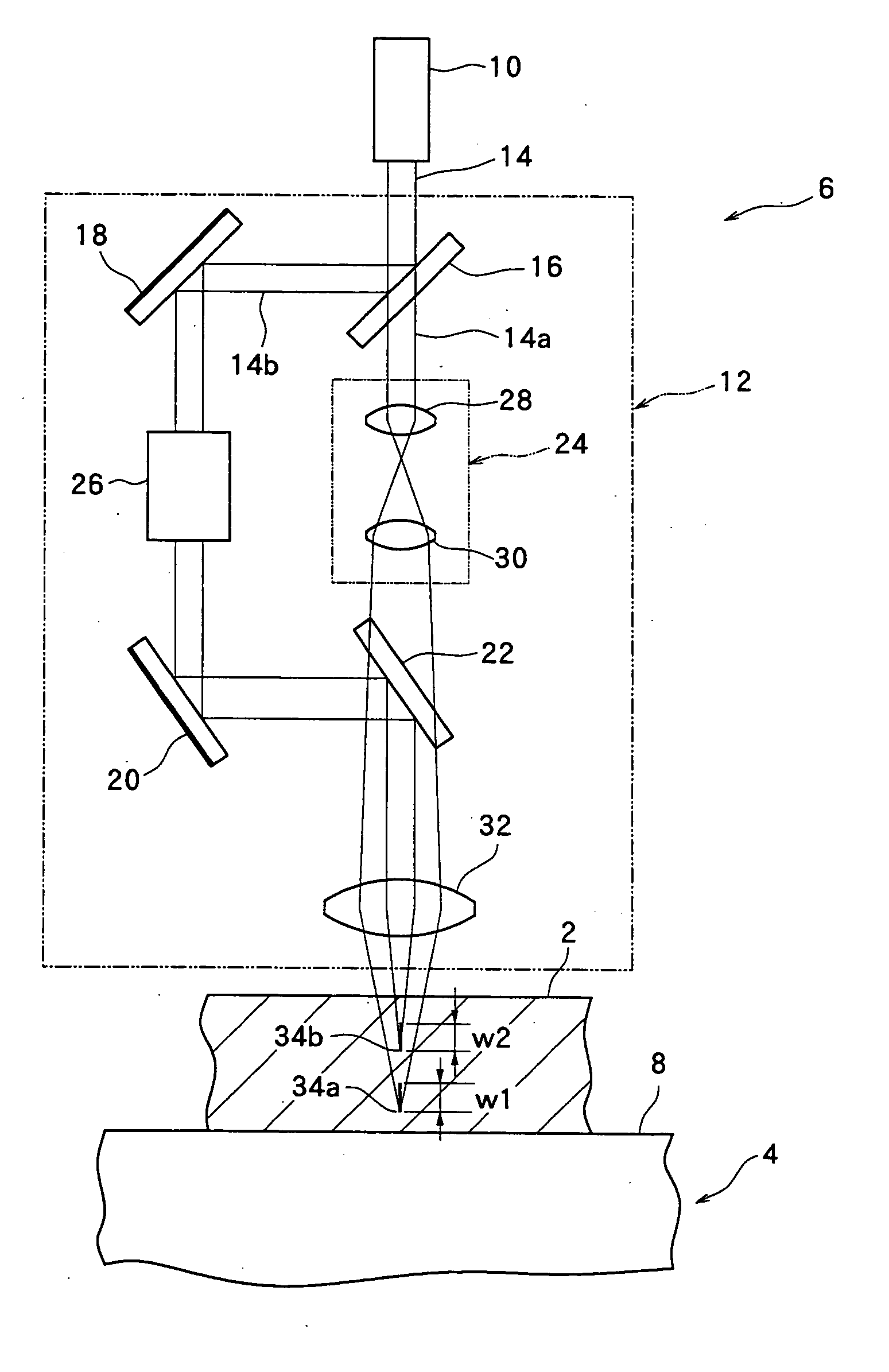
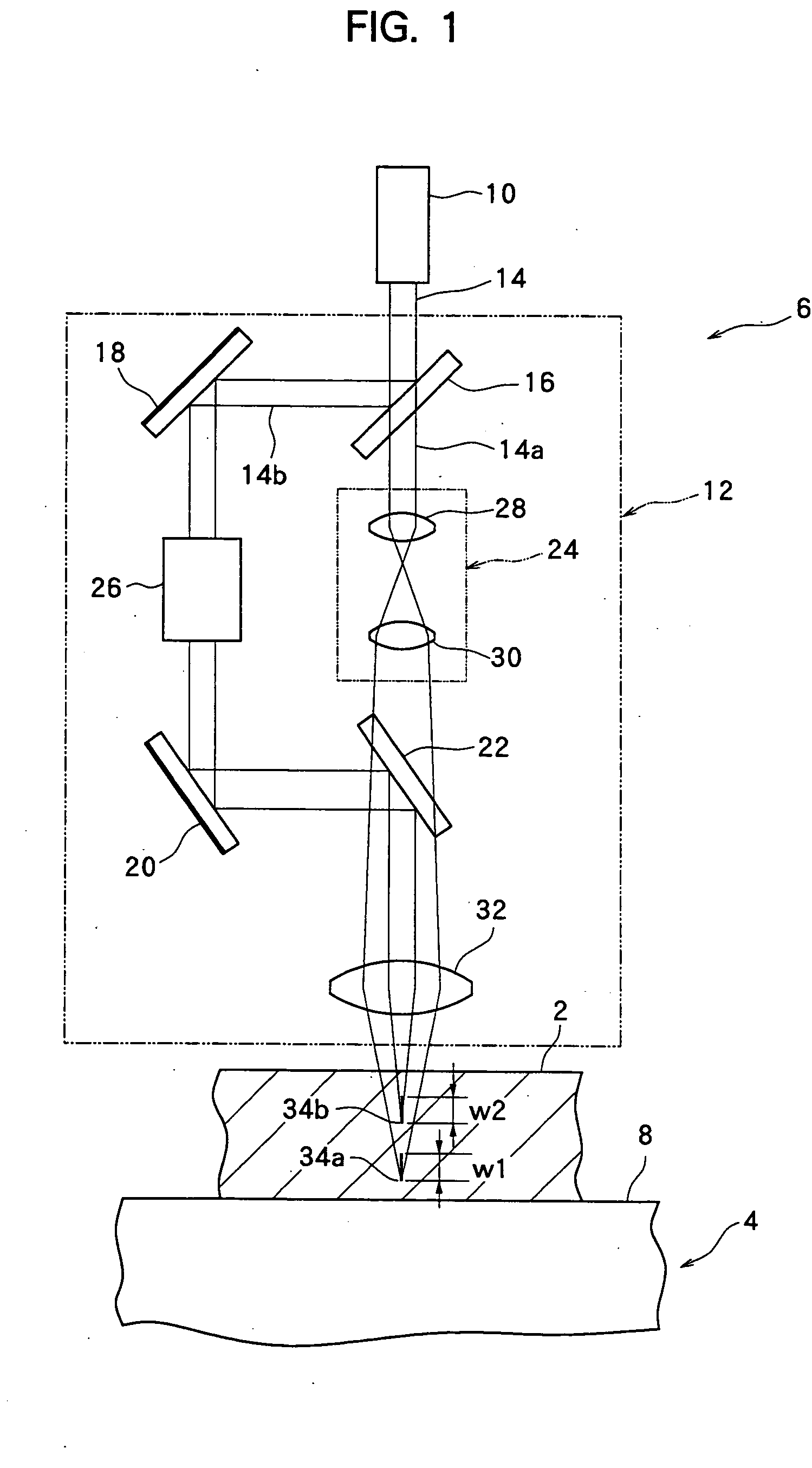
[0016]FIG. 1 schematically shows a preferred embodiment of a processing apparatus constructed in accordance with the present invention. The illustrated processing apparatus comprises holding means 4 for holding a workpiece 2, and laser beam application means indicated entirely at the numeral 6.

[0017] The holding means 4 is composed of a holding member 8 formed, for example, from a porous member or having a plurality of suction holes or grooves formed therein, and suction means (not shown) annexed to the holding member 8. The holding means 4 may be of a form in which the workpiece 2, for example, a wafer, is attracted to the surface of the holding member 8 by suction.

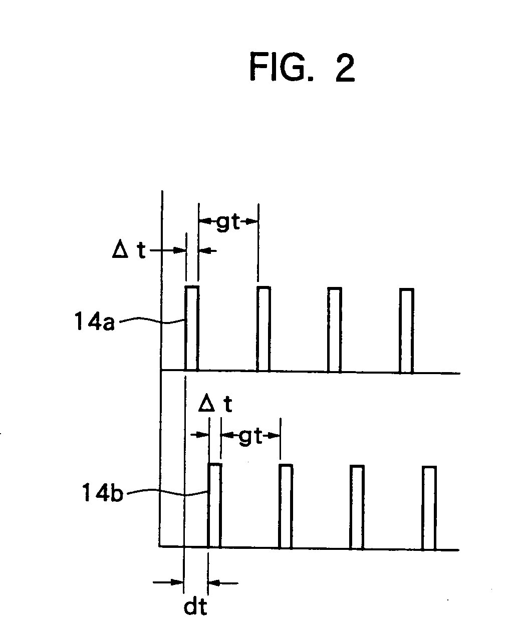
[0018] The laser beam application means 6 includes pulsed laser beam oscillation means 10, and tran...


PUM

PropertyMeasurementUnit
wavelengthaaaaaaaaaa
velocityaaaaaaaaaa
optical path length L1aaaaaaaaaa

Abstract

A processing apparatus using a laser beam, which comprises holding means for holding a workpiece, and laser beam application means for irradiating the workpiece, held by the holding means, with a pulsed laser beam capable of passing through the workpiece, thereby deteriorating the workpiece. The laser beam application means includes pulsed laser beam oscillation means and transmitting / focusing means for transmitting and focusing the pulsed laser beam oscillated by the pulsed laser beam oscillation means. The transmitting / focusing means focuses the pulsed laser beam, with a time difference provided, to at least two focus points displaced in the optical axis direction.

Description

FIELD OF THE INVENTION [0001] This invention relates to a processing apparatus using a laser beam and, more particularly, a processing apparatus comprising holding means for holding a workpiece, and laser beam application means for irradiating the workpiece, which is held by the holding means, with a pulsed laser beam capable of passing through the workpiece, thereby deteriorating the workpiece. DESCRIPTION OF THE PRIOR ART [0002] In the production of a semiconductor device, for example, it is well known that many semiconductor circuits are formed on the face of a wafer, including a suitable substrate, such as a silicon substrate, a sapphire substrate, a silicon carbide substrate, a lithium tantalate substrate, a glass substrate, or a quartz substrate, and then the wafer is divided to produce individual semiconductor circuits, namely, semiconductor devices. Various modes using a laser beam are proposed as methods for dividing the wafer. [0003] U.S. Pat. No. 6,211,488 and Japanese Pa...

Claims


Application Information

Patent Timeline
Patent Type & Authority Applications(United States)
IPC IPC(8): B23K26/067B28D5/00
CPCB23K26/0057B23K26/0613B23K26/0892B23K26/067B28D5/0011B23K26/063B23K26/0622B23K26/53
Inventor KOBAYASHI, SATOSHIMORISHIGE, YUKIO
Owner DISCO CORP
Why Eureka
Try Eureka