
Display device and electronic equipment using the same

a technology of electronic equipment and display device, which is applied in the field of display device, can solve the problems of uneven display, unfavorable use, and more serious problems of defects, and achieve the effect of reducing the uneven display of the screen

Inactive Publication Date: 2005-05-12
SEMICON ENERGY LAB CO LTD
View PDF24 Cites 17 Cited by
  • Summary
  • Abstract
  • Description
  • Claims
  • Application Information

AI Technical Summary

Benefits of technology

This approach significantly reduces display unevenness by stabilizing current flow and maintaining consistent luminance across the screen, even with variations in TFT characteristics, resulting in improved uniformity and image quality.

Problems solved by technology

Thus, even if the same voltage is input, different currents flow to OLED elements due to dispersion of performance between the OLED driving TFTs, and the fact that luminance of the pixel differs in a different location causes unevenness of display.
As a result, the emission luminance of the OLED element differs to cause unevenness of display.
This defect is a more serious problem as a panel is increased in size.

Method used


Image

  • Display device and electronic equipment using the same
  • Display device and electronic equipment using the same
  • Display device and electronic equipment using the same

Examples


embodiment 1

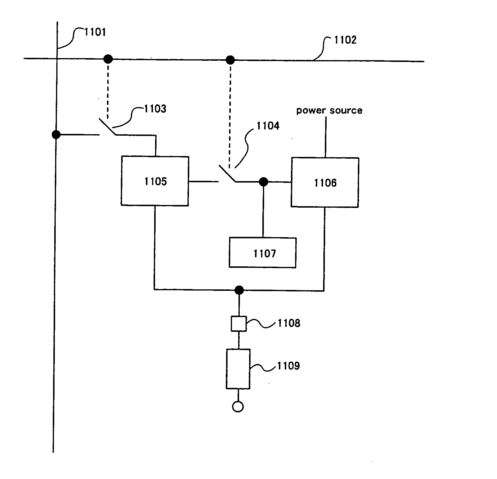
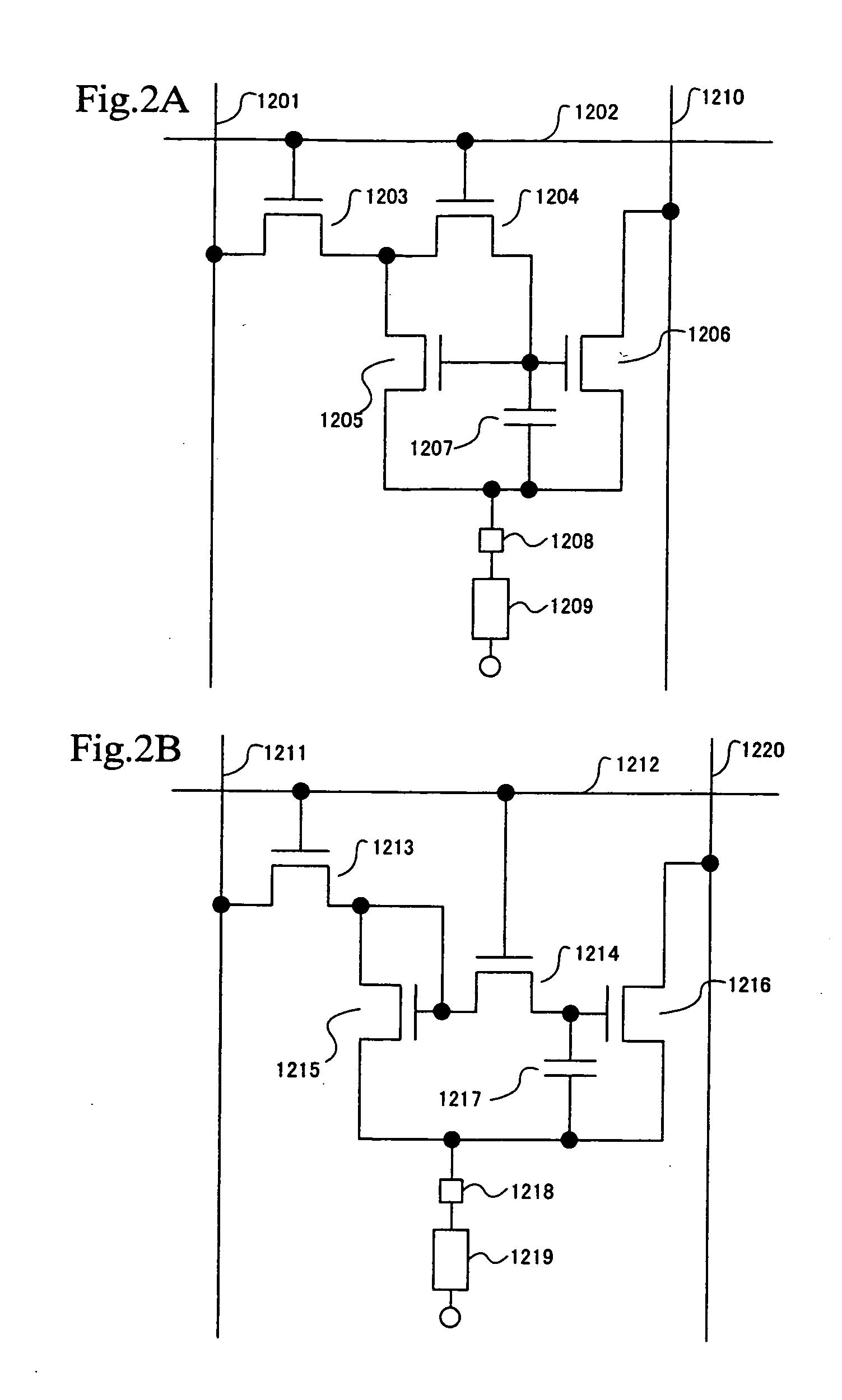
[0096]FIG. 2A shows a structure of the present invention, which is structured by thin film transistors. In this example, a current-voltage conversion element, a voltage-current conversion element, and first and second switches are structured from thin film transistors, and a holding means is structured from a capacitor.

[0097] In this embodiment, there are provided in a pixel region a source signal line 1201, a gate signal line 1202, a first switch thin film transistor 1203 which is controlled by the gate signal line and has one end connected to the source signal line 1201 and the other end connected to a drain terminal of a thin film transistor 1205, a second switch thin film transistor 1204 which has one end connected to the drain terminal of the thin film transistor 1205 and the other end connected to a gate terminal of the thin film transistor 1205, to a voltage holding capacitor 1207, and to a gate terminal of a thin film transistor 1206, a pixel electrode 1208 connected to a s...

embodiment 2

[0102]FIG. 2B shows the structure in which the connection of the switches in Embodiment 1 is changed.

[0103] In this embodiment, there are provided in a pixel region a source signal line 1211, a gate signal line 1212, a first switch thin film transistor 1213 which is controlled by the gate signal line and has one end connected to the source signal line 1211 and the other end connected to a drain terminal and a gate terminal of a thin film transistor 1215, a second switch thin film transistor 1214 which has one end connected to the drain terminal and the gate terminal of the thin film transistor 1215 and the other end connected to a voltage holding capacitor 1217 and to a gate terminal of a thin film transistor 1216, a pixel electrode 1218 connected to a source electrode of the thin film transistor 1215 and to a source electrode of the thin film transistor 1216, and a light emitting element (OLED element) 1219 which uses the pixel electrode 1218 as an anode or cathode thereof.

[0104]...

embodiment 3

[0107]FIG. 3 shows a structure in which a switch thin film transistor 1303 and a switch thin film transistor 1304 are controlled by different gate signal lines. The two gate signal lines are used, whereby timing of on and off is staggered between the switches. Thus, it becomes possible to further improve controllability.

[0108] The principle of operation is the same as in Embodiment 1, and it is possible to adopt the switch connection as shown in Embodiment 2. Further, the transistors with a single polarity can be used as the thin film transistors.


PUM


Abstract

In an active matrix EL display device, pixels which are suitable for a constant current drive are structured. The pixel includes a first switch which has one end connected to a source signal line and the other end connected to a current-voltage conversion element, a second switch which has one end connected to the current-voltage conversion element and the other end connected to a voltage holding capacitor and to a voltage-current conversion element, and a pixel electrode connected to the current-voltage conversion element and to the voltage-current conversion element.

Description

BACKGROUND OF THE INVENTION [0001] 1. Field of the Invention [0002] The present invention relates to a display device, particularly, to an OLED display device using a thin film transistor formed on the transparent substrate such as glass or plastic. Further, it relates to an electronic device using the display device. [0003] 2. Description of the Related Art [0004] In resent years, a cellular phone has been becoming popular by developing communication technology. In future, electrical transmission of moving pictures and transmission of a large quantity of information will be expected. With being lightened, a mobile personal compute is into production. An information device called a personal digital assistant (PDA) developed from electrical books is produced and becoming popular. With developing a display device and the like, most of such portable information devices are equipped with flat displays. [0005] The latest technology aims at using an active matrix display device as a displ...

Claims


Application Information

Patent Timeline
Patent Type & Authority Applications(United States)
IPC IPC(8): G09G3/20G09G3/32
CPCG09G3/2011G09G3/2014G09G3/2018G09G3/2022G09G3/3241G09G2320/0233G09G2300/0814G09G2300/0842G09G2310/0251G09G2310/0262G09G2320/0219G09G2300/0426
Inventor KOYAMA, JUN
Owner SEMICON ENERGY LAB CO LTD
Learn More