Semiconductor device having overcurrent protection function and data setting method thereof

a technology of overcurrent protection and semiconductor devices, which is applied in the direction of electronic switching, pulse technique, power conversion systems, etc., can solve the problems of difficult to change the overcurrent detection level, the temperature dependence of the diversion ratio has reached an unignorable level, and the inability to accurately implement overcurrent protection in the conventional ipm

Inactive Publication Date: 2005-05-12
MITSUBISHI ELECTRIC CORP
View PDF14 Cites 61 Cited by
  • Summary
  • Abstract
  • Description
  • Claims
  • Application Information

AI Technical Summary

Benefits of technology

[0013] It is an object of the present invention to provide a semiconductor device with an overcurrent protection function for a switching element such as an IPM wherein the situation that an overcurrent detection level varies in dependence on temperature can be remedied and the setting of the overcurrent detection level can be easily changed.
[0015] Since the reference level for overcurrent detection is adjusted based on the temperature of the switching element measured by the temperature measuring portion, the situation that the overcurrent detection level varies in dependence on temperature is remedied. Further, in comparison with the case of Japanese Patent Application Laid-Open No. 2003-009509 where the operation coefficient in the correction circuit is reset, the setting of the overcurrent detection level can be easily changed. Furthermore, in comparison with the case of Japanese Patent Application Laid-Open No. 2003-009509 where the measured current value is corrected by the correction circuit, reduction of the circuit size can be achieved.
[0017] By changing the temperature of the semiconductor device and providing the main current equivalent to the overcurrent level to the switching element, data of a new reference level is automatically created. Therefore, a user does not have to prepare new reference level data in advance. Further, even if the procedure is conducted manually, no individual differences or errors occurs in measurement results. Therefore, an improved reliability of the semiconductor device is realized.

Problems solved by technology

Especially, in recent years, current capacity of IGBTs have been increased and IGBTs have been miniaturized in order to suppress switching losses that accompany the increased current capacity, the temperature dependence of the diversion ratio has reached an unignorable level.
Therefore, it is difficult to precisely detect the overcurrent and thus it is difficult to accurately implement overcurrent protection in the conventional IPM.
In a conventional IPM, it is difficult to change the overcurrent detection level once it is set.
In this case, individual differences or errors might occur in measurement results.
This is problematic leading to enlarged circuit size.

Method used


Image

  • Semiconductor device having overcurrent protection function and data setting method thereof
  • Semiconductor device having overcurrent protection function and data setting method thereof
  • Semiconductor device having overcurrent protection function and data setting method thereof

Examples


Embodiment Construction

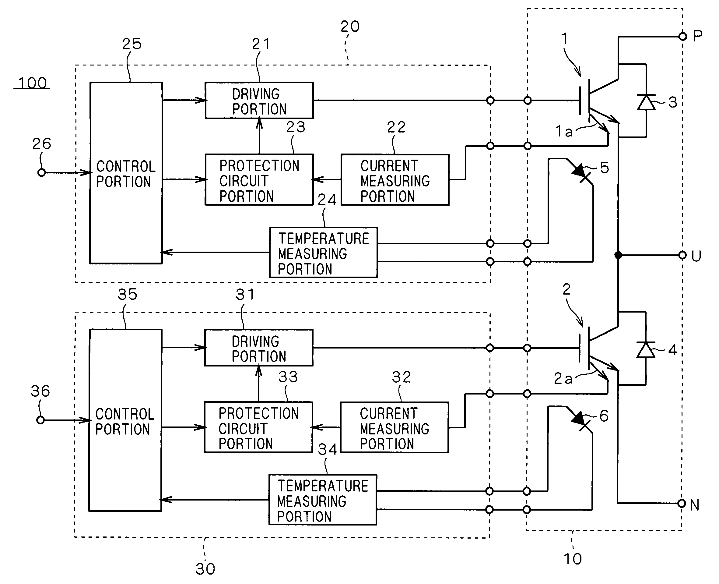
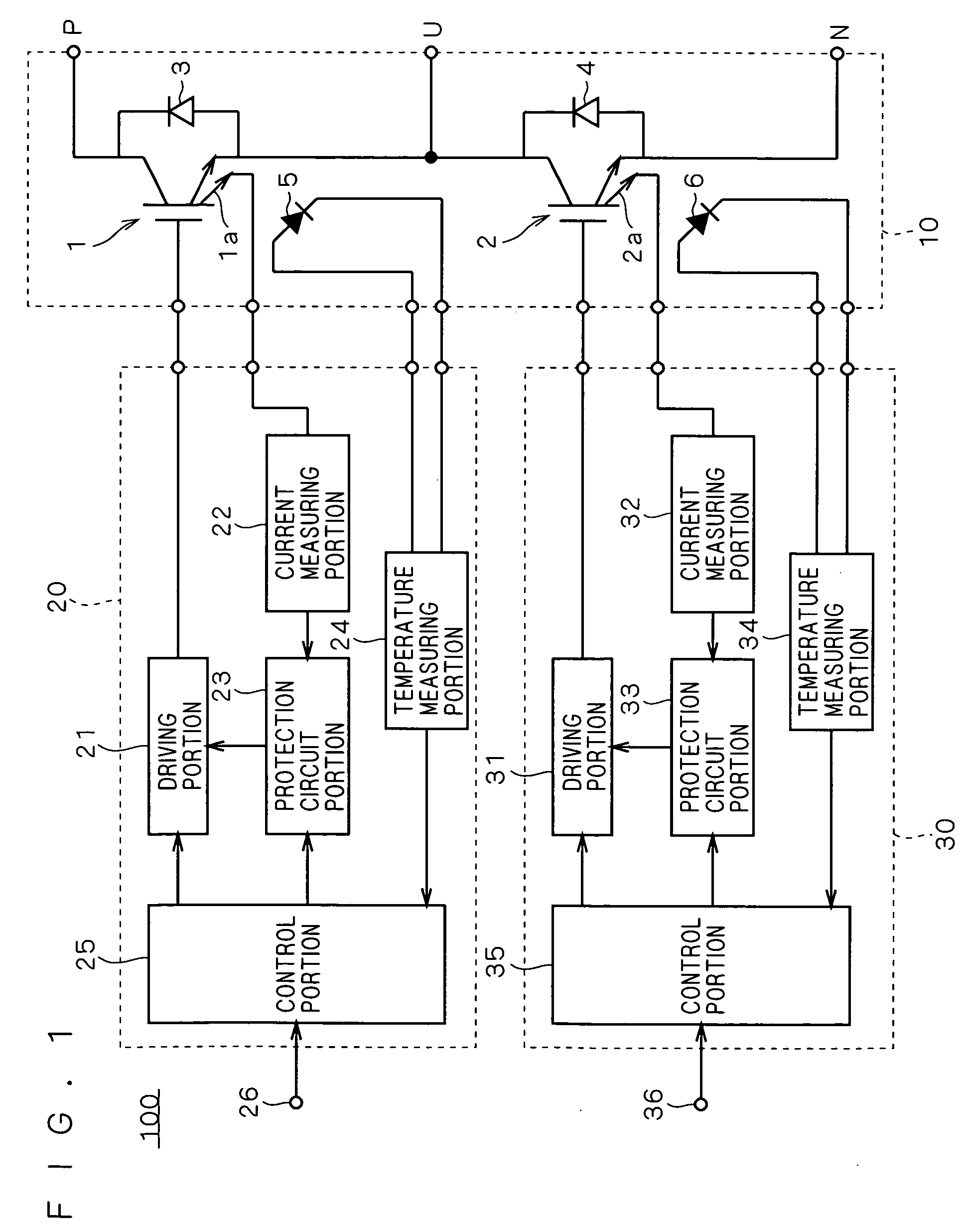
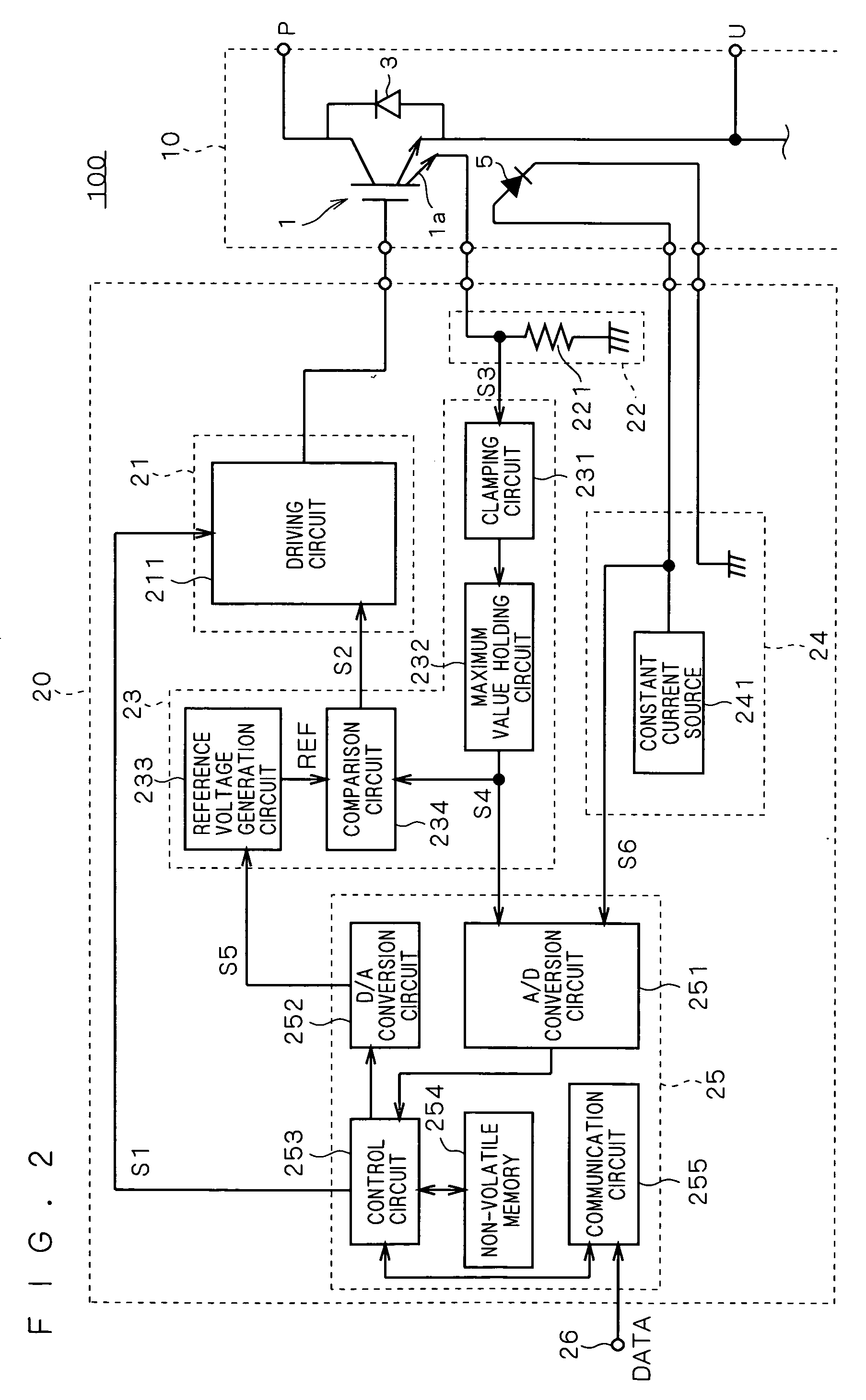
[0024]FIG. 1 shows the structure of an IPM semiconductor device according to a preferred embodiment of the present invention. An IPM 100 comprises an inverter 10 and driving devices 20 and 30 for driving the inverter 10. The inverter 10 comprises two switching elements connected in series to each other, namely, an IGBT 1 on the P side and an IGBT 2 on the N side, each serving as an output element for driving a load (not shown). The IGBTs 1 and 2 are provided with sense electrodes 1a and 1b, respectively, where a sense current proportionate to a main current (a collector current) flows therethrough. The IPM 100 further comprises free-wheeling diodes 3 and 4, connected to the IGBTs 1 and 2, respectively, and temperature measuring diodes 5 and 6 for measuring respective temperatures of the IGBTs 1 and 2.

[0025] The driving device 20 drives the IGBT 1 and is provided with an overcurrent protection function for preventing an overcurrent from flowing through the IGBT 1. The driving device...


PUM


Abstract

In a driving device (20) for driving an IGBT (1), a current measuring portion (22) measures a main current amount flowing through the IGBT (1). When the main current amount measured by the current measuring portion (22) reaches a predetermined reference level, a protection circuit portion (23) limits the main current at the IGBT (1) to protect it. A temperature measuring portion (24) measures the temperature of the IGBT (1). The control portion (25) adjusts the aforementioned reference level based on the temperature of the IGBT (1) measured by the temperature measuring portion (24). A control portion (35) stores setting values of the reference level as data.

Description

BACKGROUND OF THE INVENTION [0001] 1. Field of the Invention [0002] This invention relates to a semiconductor device suitable for use in a power converter such as an inverter. More particularly, this invention relates to an improvement to realize reduced or eliminated temperature dependence in an overcurrent detection function. [0003] 2. Description of the Background Art [0004] A semiconductor device for driving a switching element such as an insulated gate bipolar transistor (IGBT) element and having an overcurrent detection function to detect a current exceeding a predetermined limit (an overcurrent) flowing through the switching element is generally used in a power converter such as an inverter. A semiconductor device with such a function and further having a protection function to limit a main current based on an overcurrent detection result (an overcurrent protection function) is known as an intelligent power module (hereinafter referred to as an “IPM”). The IPM is especially s...

Claims


Application Information

Patent Timeline
Patent Type & Authority Applications(United States)
IPC IPC(8): H02M1/00H02H3/08H02M1/08H03K17/08H03K17/082H03K17/14H03K17/56
CPCH03K2017/0806H03K17/0828
Inventor KUMAGAI, TOSHIYUKI
Owner MITSUBISHI ELECTRIC CORP
Why Eureka
Try Eureka