Frame attaching process
- Summary
- Abstract
- Description
- Claims
- Application Information
AI Technical Summary
Benefits of technology
Problems solved by technology
Method used
Image
Examples
Embodiment Construction
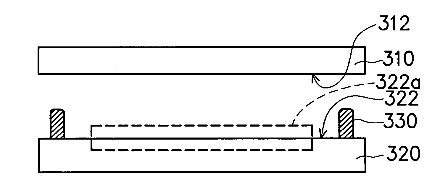
[0023] Please referring to FIGS. 3A-3D, they are a schematic process flow showing a first exemplary frame attaching process in accordance with the present invention.
[0024] As shown in FIG. 3A, a transparent substrate 310 and a chip 320 are provided. The transparent substrate 310 has an attaching surface 312 and the transparent substrate 310 can be made of, for example, glass or the other transparent material. The chip 320 is one of chips within an un-sawed wafer. In addition, each chip 320 has an active area 322 and the active area 322 has a functional area 322a thereon. When chip 320 is a chip with optical-electronic function, the functional area 322a can sense light or illuminate.
[0025] As shown in FIG. 3B, a frame 330 is formed on the active area 322 of the chip 320, and the frame 330 surrounds the functional area 322a.
[0026] As shown in FIG. 3C, a negative pressure is provided, which ranges from about 0.5 to about 0.9 atmospheres. The negative pressure is generated from, for ...
PUM
| Property | Measurement | Unit |
|---|---|---|
| Pressure | aaaaa | aaaaa |
| Transparency | aaaaa | aaaaa |
Abstract
Description
Claims
Application Information


