Scan chain registers that utilize feedback paths within latch units to support toggling of latch unit outputs during enhanced delay fault testing

a technology of latch unit output and feedback path, applied in the field of integrated circuit devices, can solve problems such as limiting the effectiveness of scan chain circuits

Active Publication Date: 2005-05-19
INTEGRATED DEVICE TECH INC
View PDF64 Cites 29 Cited by
  • Summary
  • Abstract
  • Description
  • Claims
  • Application Information

AI Technical Summary

Benefits of technology

[0005] Embodiments of the present invention include an integrated circuit device that utilizes a scan chain register to support efficient reliability testing of internal circuitry that is not readily accessible from the I / O pins of the device. This reliability testing includes the performance of, among other things, delay fault and stuck-at fault testing of elements within the internal circuitry. According to some of these embodiments, an integrated circuit device is provided with a scan chain register having a plurality of scan chain latch units therein that support a toggle mode of operation. The scan chain register is provided with serial and parallel input ports and serial and parallel output ports. Each of the plurality of scan chain latch units includes a latch element and additional circuit elements that are configured to selectively establish at least one feedback path in the respective latch unit. This feedback path can operate to pass an inversion of a signal at an output of the latch to an input of the latch when the corresponding scan chain latch unit is enabled to support the toggle mode of operation. Accordingly, if the output of the latch is set to a logic 1 level, then a toggle operation will cause the output of the latch to automatically switch to a logic 0 level and vice versa. Because of the presence of a respective feedback path within each scan chain latch unit, the toggle operation at the output of a scan chain latch unit will be independent of the value of any other output of any other scan chain latch unit within the scan chain.

Problems solved by technology

This functional dependency between the output of one shift register latch and the output of a preceding shift register latch during the fault test operation can limit the effectiveness of the scan chain circuit 110 when testing for other more complicated types of delay faults within an integrated circuit device.

Method used


Image

  • Scan chain registers that utilize feedback paths within latch units to support toggling of latch unit outputs during enhanced delay fault testing
  • Scan chain registers that utilize feedback paths within latch units to support toggling of latch unit outputs during enhanced delay fault testing
  • Scan chain registers that utilize feedback paths within latch units to support toggling of latch unit outputs during enhanced delay fault testing

Examples


Embodiment Construction

[0026] The present invention will now be described more fully hereinafter with reference to the accompanying drawings, in which preferred embodiments of the invention are shown. This invention may, however, be embodied in many different forms and should not be construed as limited to the embodiments set forth herein. Rather, these embodiments are provided so that this disclosure will be thorough and complete, and will fully convey the scope of the invention to those skilled in the art. Like numbers refer to like elements throughout. The suffix B or prefix symbol “ / ” to a signal name may denote a complementary data or information signal or an active low control signal, for example.

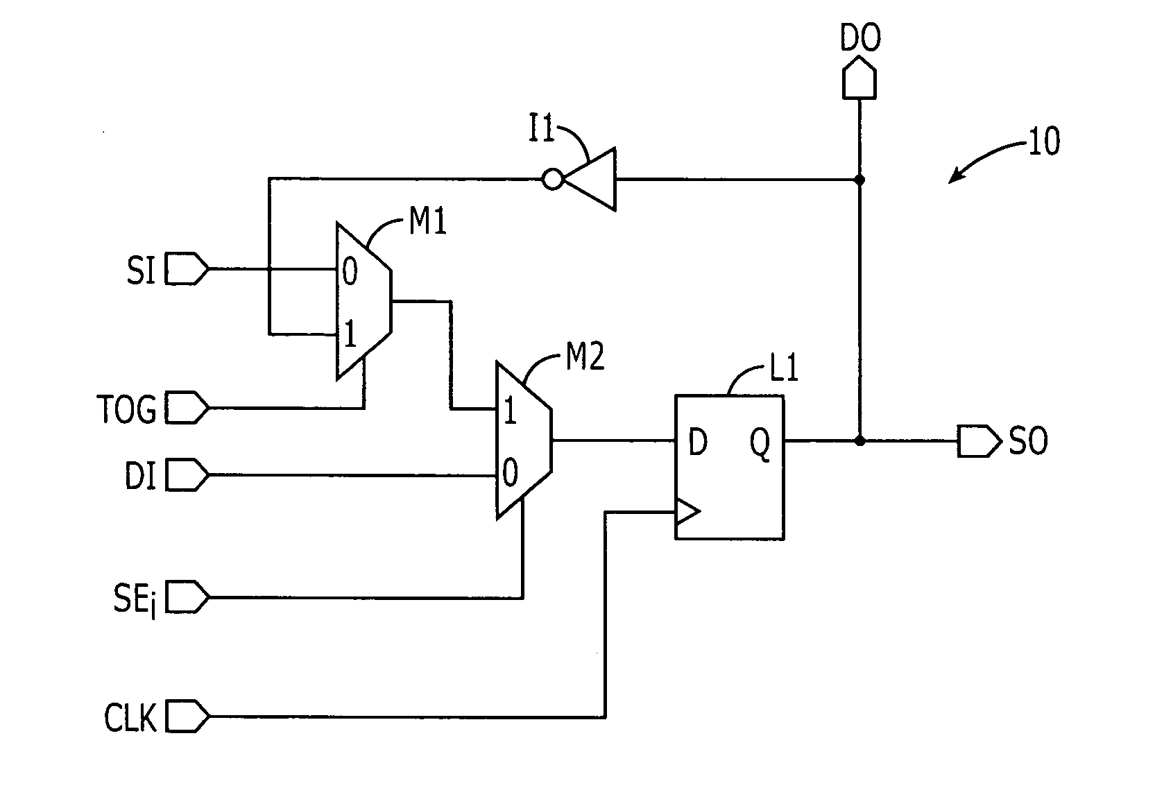
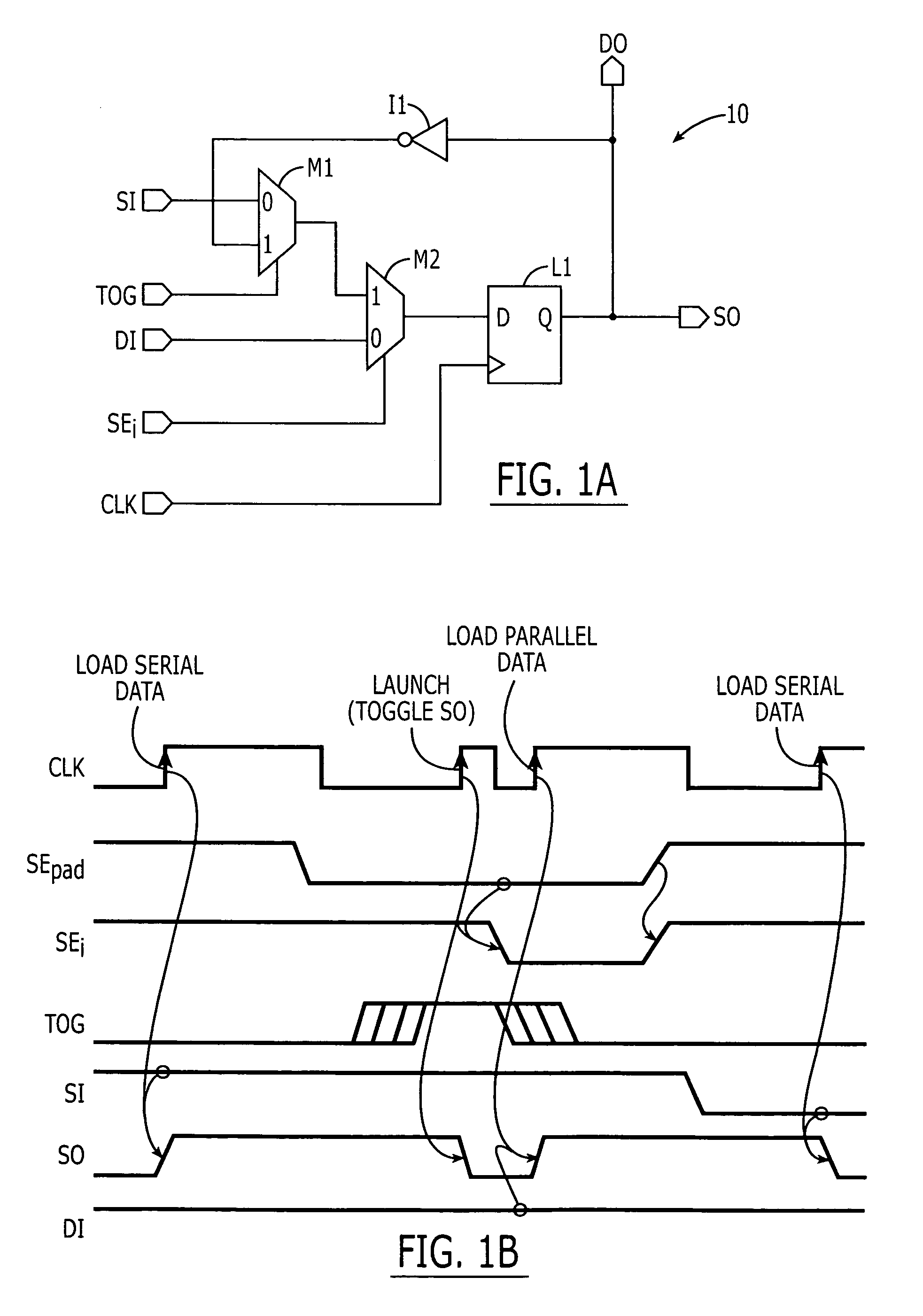
[0027] Referring now to FIG. 1A, a scan chain latch unit 10 according to an embodiment of the present invention is illustrated as including first and second multiplexers M1 and M2, a latch L1 and an inverter I1. The latch L1 is shown as a D-type flip-flop having an input D and a “true” output Q that is fed...


PUM


Abstract

An integrated circuit device utilizes a serial scan chain register to support efficient reliability testing of internal circuitry that is not readily accessible from the I/O pins of the device. This reliability testing includes the performance of, among other things, delay fault and stuck-at fault testing of elements within the internal circuitry. The scan chain register has scan chain latch units that support a toggle mode of operation. The scan chain register is provided with serial and parallel input ports and serial and parallel output ports. Each of the plurality of scan chain latch units includes a latch element and additional circuit elements that are configured to selectively establish a feedback path in the respective latch unit. This feedback path operates to pass an inversion of a signal at an output of the latch to an input of the latch when the corresponding scan chain latch unit is enabled to support a toggle mode of operation. Thus, if the output of the latch is set to a logic 1 level, then a toggle operation will cause the output of the latch to switch to a logic 0 level and vice versa. Because of the presence of a respective feedback path within each scan chain latch unit, the toggle operation at the output of a scan chain latch unit will be independent of the value of any other output of other scan chain latch units within the scan chain.

Description

REFERENCE TO RELATED APPLICATION [0001] This application claims priority to U.S. Provisional Application Ser. No. 60 / 520,213, filed Nov. 14, 2003, the disclosure of which is hereby incorporated herein by reference.FIELD OF THE INVENTION [0002] The present invention relates to integrated circuit devices and methods of operating same, and more particularly to integrated circuit devices that utilize scan chains to facilitate device testing. BACKGROUND OF THE INVENTION [0003] Scan design test techniques are frequently used to facilitate testing of complicated integrated circuit devices. A variety of these techniques are disclosed in U.S. Pat. Nos. 6,453,456 and 6,490,702. In particular, FIG. 10 of the '702 patent discloses a scan chain circuit 110 that purports to solve a latch adjacency problem when testing for delay faults within an integrated circuit. This scan chain circuit 110 includes a plurality of shift register latches 30 that operate as stages within the scan chain circuit 110...

Claims


Application Information

Patent Timeline
Patent Type & Authority Applications(United States)
IPC IPC(8): G01R31/3185
CPCG01R31/31858G01R31/318541
Inventor WONG, TAK KWONG
Owner INTEGRATED DEVICE TECH INC
Why Eureka
Try Eureka