
Self-trim and self-test of on-chip values

a technology of analog values and self-testing, which is applied in the direction of automatic frequency control, pulse automatic control, electrial characteristics varying frequency control, etc., can solve the problems of consuming valuable test time, needing to trim the values produced by analog circuitry, and chip that might not function properly

Active Publication Date: 2012-03-27
DIALOG SEMICONDUCTOR GMBH
View PDF21 Cites 2 Cited by
  • Summary
  • Abstract
  • Description
  • Claims
  • Application Information

AI Technical Summary

Benefits of technology

[0008]It is an objective of the present invention to provide a self-trim capability, which produces a trimmed circuit under trim (CUT) where the trimming process is independent of the ATE and allows testing not related to the CUT to proceed in parallel with the trimming process.

Problems solved by technology

Imperfection in the manufacture of the chips containing the integrated circuits results in the need to trim the values produced by the analog circuitry to produce a chip that might not function properly as designed.
The trim operation is performed in series with further testing of the integrated circuit and consumes valuable test time.

Method used


Image

  • Self-trim and self-test of on-chip values
  • Self-trim and self-test of on-chip values
  • Self-trim and self-test of on-chip values

Examples


Embodiment Construction

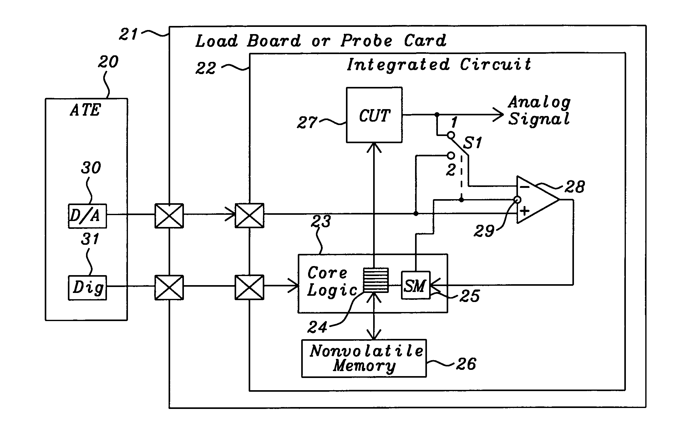
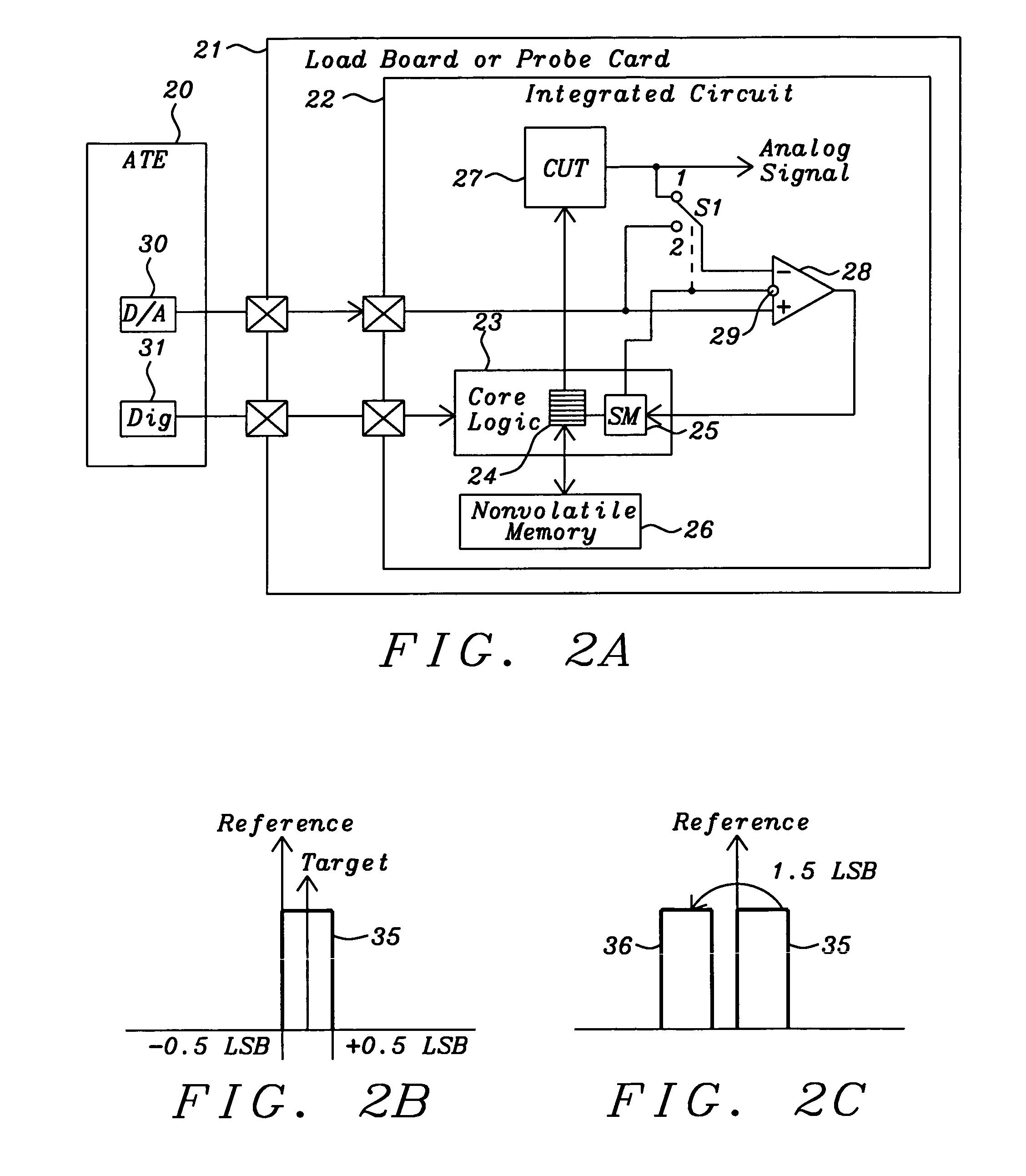
[0023]In FIG. 2A is shown a block diagram of the digital self-test and self-trim circuitry of the present invention. An ATE 20 is connected to a load board or probe card 21 which is connected to an integrated circuit under test 22. The ATE connects an analog reference signal to the integrated circuit chip from a D / A converter circuit 30, and a digital signal connected to core logic 23 through a Dig driver 31. The D / A converter 30 in the ATE 20 couples an analog reference signal to a comparator 28 within the integrated circuit 22 under trim and test. The core logic comprises a register stack 24 for holding digital data from the ATE and a state machine (SM) 25 for controlling self-test and self-trim operations. A nonvolatile memory 26 is connected to the register stack to store a final trim value to be used to control the analog output of the circuit under trim (CUT) 27 once trimming of the CUT has been completed. A comparator circuit 28 comprises an offset input 29 controlled by the ...


PUM


Abstract

A self-trim circuit provides a technique to trim a CUT (circuit under trim) using a LSB offset to determine the best digital value to trim the CUT. The self-trim circuit is also used to self-test the digital and analog portions of the self-trim circuitry, whereby the existence of a digital stuck at fault condition is detected. A state machine controls a digital stack to couple digital trim data to the CUT and read the output of a comparator circuit that signifies when a proper digital trim value has been used. Thereafter the proper digital trim value is stored into a nonvolatile memory.

Description

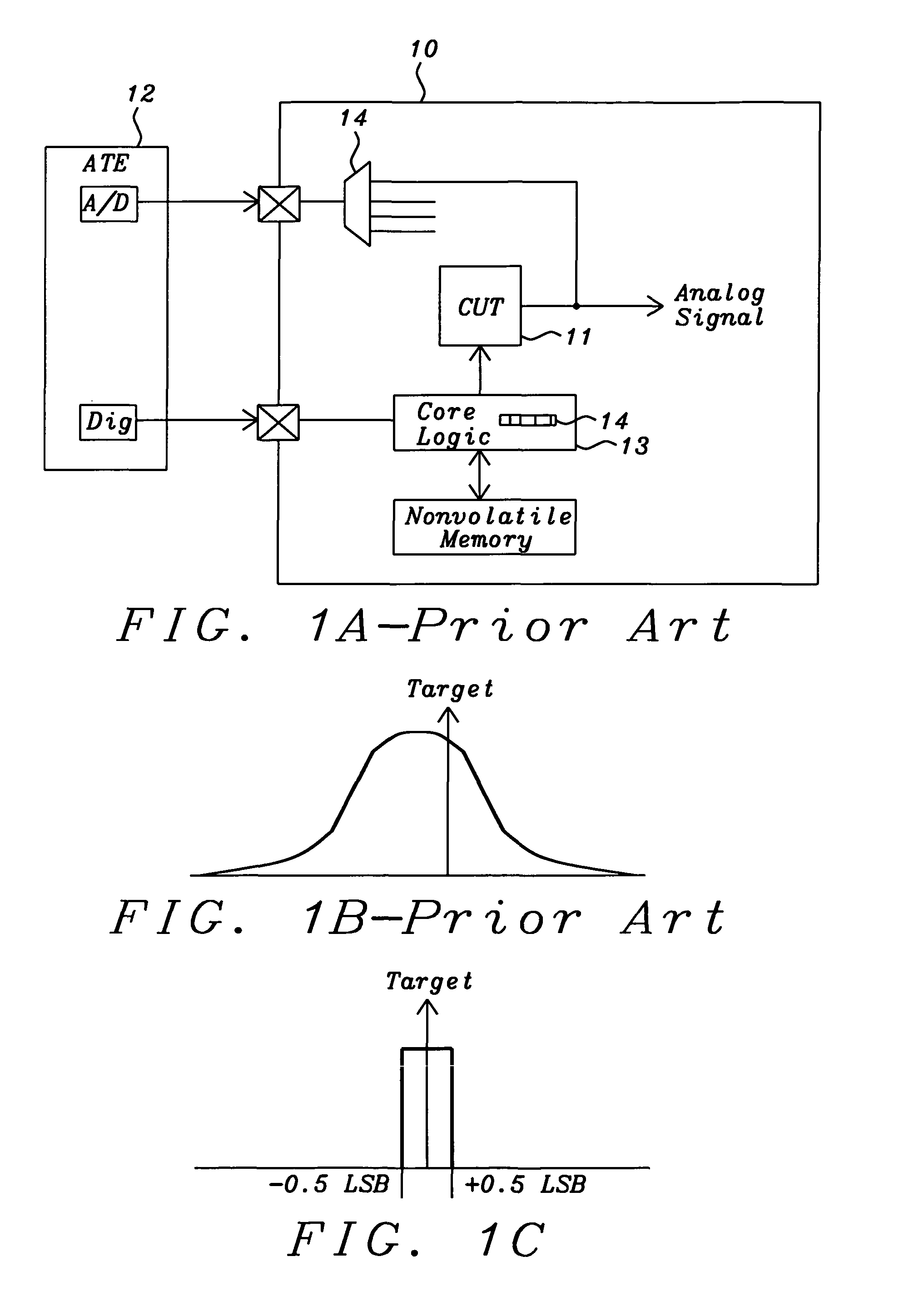
BACKGROUND OF THE INVENTION[0001]1. Field of Invention[0002]The present invention is related to calibration and testing of semiconductor chips and in particular to the self-trimming and self-testing of on-chip analog values.[0003]2. Description of Related Art[0004]Integrated circuits use a wide collection of analog circuitry to enable the function of the integrated circuits ranging from reference voltages to reference currents, offsets, comparator thresholds and oscillator frequencies. Imperfection in the manufacture of the chips containing the integrated circuits results in the need to trim the values produced by the analog circuitry to produce a chip that might not function properly as designed. When performing multi-site testing, for instance semiconductor chips on a wafer, trimming cannot be done in parallel because the ATE (automatic test equipment) must react to the individual behavior of circuits on the various chips, individually calculate trim values and then send these val...

Claims


Application Information

Patent Timeline
Patent Type & Authority Patents(United States)
IPC IPC(8): H03L7/085
CPCG01R31/31903G01R31/31915G01R31/31932
Inventor VON STAUDT, HANS MARTINHUL.BETA., ROLFKELLER, MICHAELBURKHARDT, HELMUT
Owner DIALOG SEMICONDUCTOR GMBH
Learn More