On-chip stuck-at fault detector and detection method

a fault detector and chip technology, applied in the field of integrated circuit devices, can solve problems such as the problem of more problematic testing of such designs in fpgas that are partially programmabl

Inactive Publication Date: 2011-01-04
XILINX INC
View PDF9 Cites 3 Cited by
  • Summary
  • Abstract
  • Description
  • Claims
  • Application Information

AI Technical Summary

Benefits of technology

[0013]In accordance with a third embodiment of the invention, a method of on-chip stuck-at fault detection in an integrated circuit using a test circuit for critical path testing can include the steps of generating a data signal using a sequence circuit having a first sequence circuit and a second sequence circuit to sensitize a critical path between a source sequential circuit and a destination sequential circuit, capturing an output from the destination sequential circuit at an analyzer circuit, comparing a signa

Problems solved by technology

However, as partially programmable parts may be used for some designs, testing of

Method used


Image

  • On-chip stuck-at fault detector and detection method
  • On-chip stuck-at fault detector and detection method
  • On-chip stuck-at fault detector and detection method

Examples


Embodiment Construction

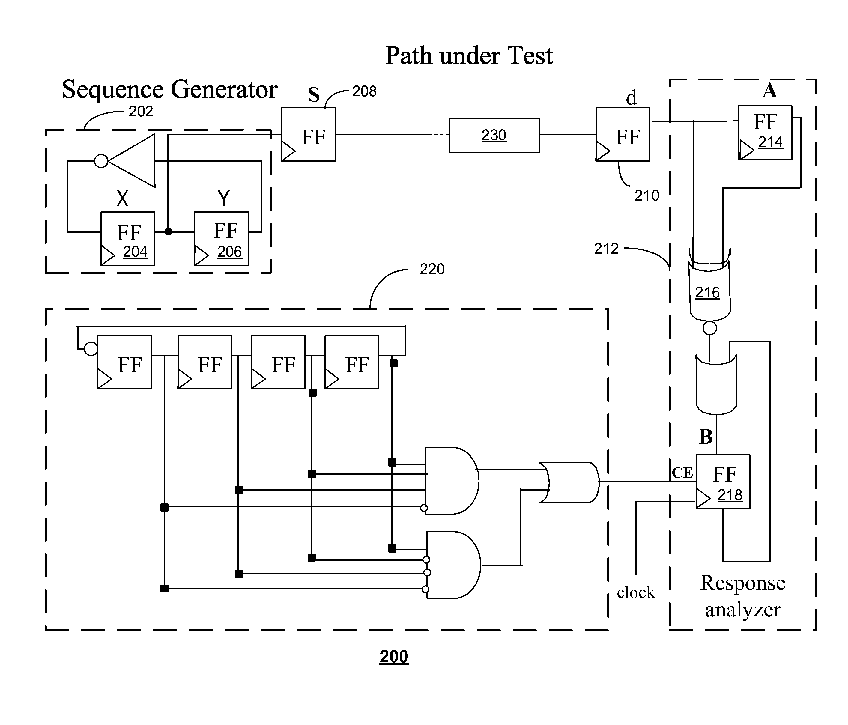
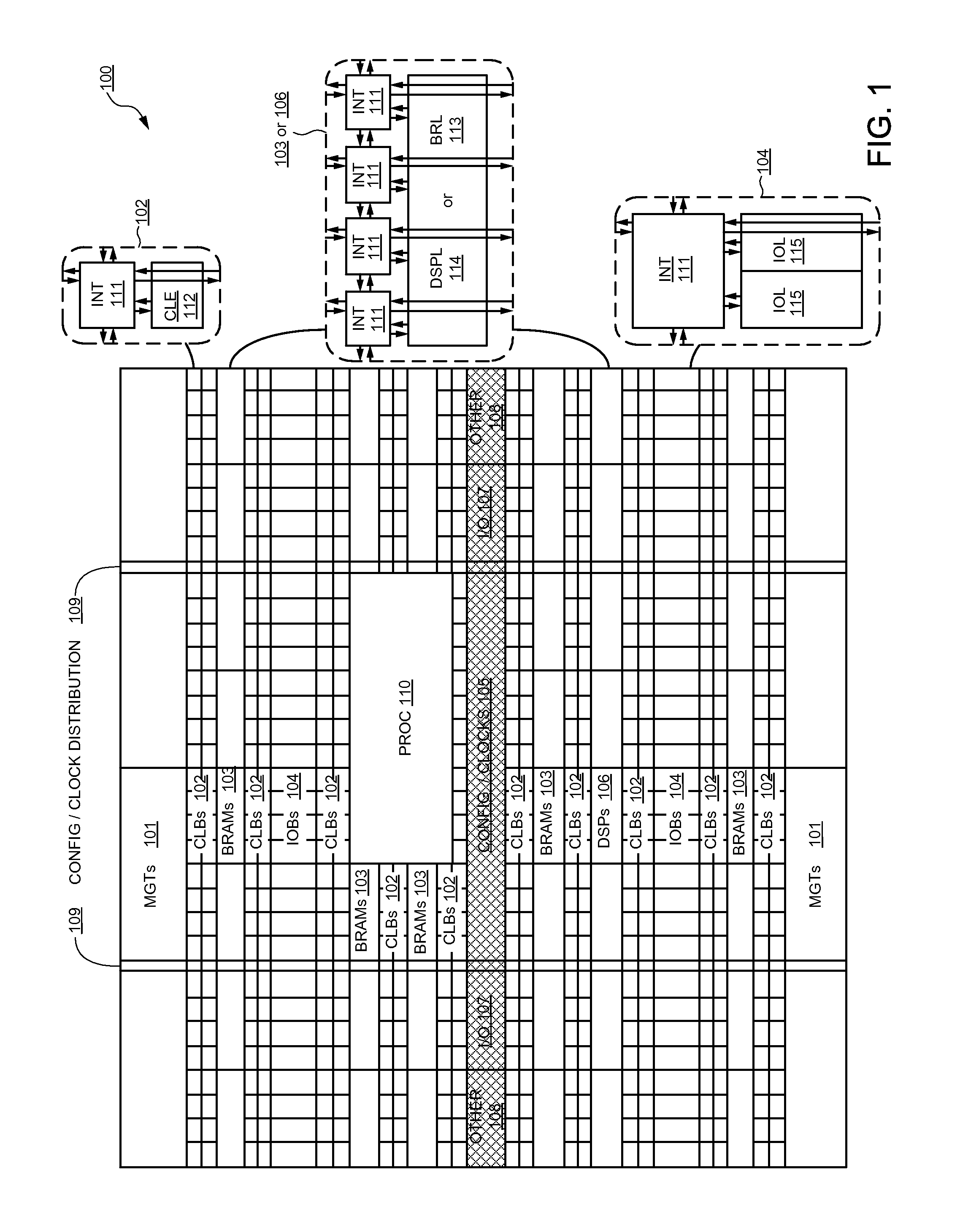
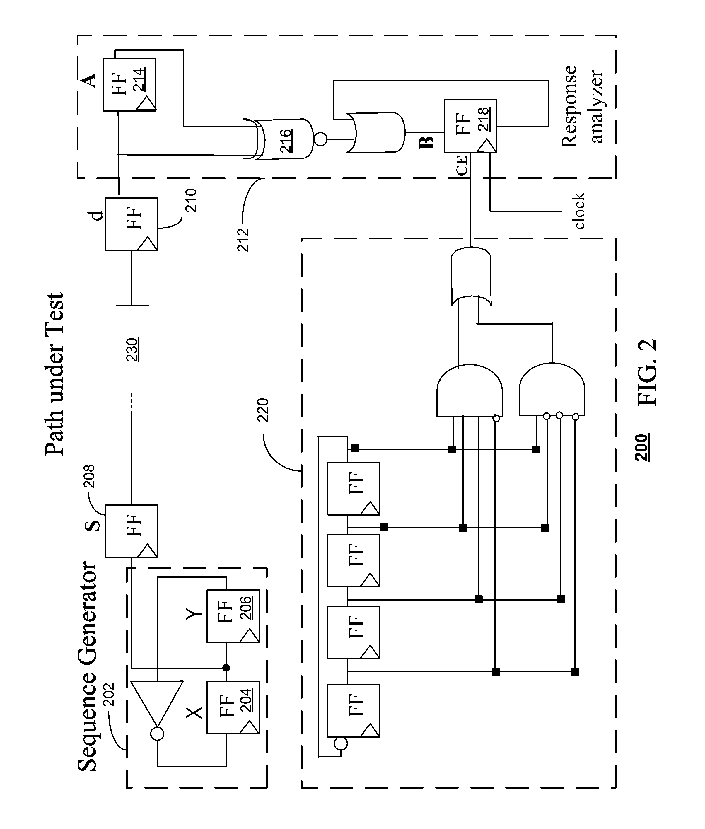
[0020]In the following description, numerous specific details are set forth to provide a more thorough description of the specific embodiments of the invention. It should be apparent, however, to one skilled in the art, that the invention may be practiced without all the specific details given below. In other instances, well known features have not been described in detail so as not to obscure the invention. For ease of illustration, the same number labels are used in different diagrams to refer to the same items; however, in alternative embodiments the items may be different.

[0021]Embodiments of the present invention are applicable to many types of integrated circuits, especially those including programmable logic. However, examples of some embodiments of the present invention are described in relation to application in Field Programmable Gate Arrays (FPGAs). These exemplary descriptions are not intended to limit embodiments of the present invention, but to illuminate them in the c...


PUM


Abstract

An on-chip stuck-at fault detector in an integrated circuit using a test circuit for critical path testing can include a sequence circuit having a first sequential circuit and a second sequential circuit to sensitize the critical path between a source sequential circuit and a destination sequential circuit, an analyzer circuit for capturing an output from the destination sequential circuit and comparing a signal between the destination sequential circuit and the analyzer circuit at predetermined clock cycles, and a controller for strobing the analyzer circuit at the predetermined clock cycles. The first sequence and second circuits can both be initialized to a zero mode (e.g., x=0 and y=0). Thus, no stuck-at faults are determined if the destination sequential circuit and an analyzer sequential circuit in the analyzer circuit have different values and a zero result is captured at a sticky-bit flip flop.

Description

FIELD OF THE INVENTION[0001]The invention relates to integrated circuit devices (ICs). More particularly, the invention relates to a test circuit for verifying a critical path for an IC.BACKGROUND OF THE INVENTION[0002]Programmable logic devices (PLDs) are a well-known type of integrated circuit that can be programmed to perform specified logic functions. One type of PLD, the field programmable gate array (FPGA), typically includes an array of programmable tiles. These programmable tiles can include, for example, input / output blocks (IOBs), configurable logic blocks (CLBs), dedicated random access memory blocks (BRAM), multipliers, digital signal processing blocks (DSPs), processors, clock managers, delay lock loops (DLLs), and so forth. As used herein, note that the terms “include” and “including” mean including without limitation.[0003]Each programmable tile typically includes both programmable interconnect and programmable logic. The programmable interconnect typically includes a...

Claims


Application Information

Patent Timeline
IPC IPC(8): G01R31/3177G01R31/40
CPCG01R31/31725G01R31/318516
Inventor JAIRAM, PRABHAVERMA, HIMANSHU J.
Owner XILINX INC
Why Eureka
Try Eureka