Circuit designing program and circuit designing system having function of test point insetion

a circuit design and circuit technology, applied in the direction of instruments, nuclear elements, nuclear engineering, etc., can solve the problems of failure analysis becoming more difficult, failure analyzers lacking resolution for the element size of the integrated circuit, and the possibility of including defective products in the produced products at some percentages, so as to improve fault analyzability

Inactive Publication Date: 2008-04-17
RENESAS ELECTRONICS CORP
View PDF10 Cites 3 Cited by
  • Summary
  • Abstract
  • Description
  • Claims
  • Application Information

AI Technical Summary

Benefits of technology

[0036]According to the present invention, the probability of the fault candidate number allowed to be narrowed down at least up to the designated number at an occurrence when a fault takes place will get higher. Consequently, the fault analyzability is improved.

Problems solved by technology

In the field of semiconductor integrated circuits, there is a possibility of including defective products in the produced products at some percentages.
However, in the recent years, as the microtechnology is applied to semiconductor integrated circuits more, failure analysis is becoming more difficult.
A reason thereof is that a failure analyzer is lacking resolution for the element size in the integrated circuit.
Such an optical failure analyzer uses long-wavelength light in the infra-red region and cannot obtain resolution not more than several tenths of a micron due to influence of the diffractive limit.
Therefore, the EB analyzer is hardly applicable as well.
However, in the case where the fault sites include a lot of equivalent faults, fault diagnosis cannot specify the true fault sites but a plurality of fault candidates will be extracted.
However, a number of fault candidates occasionally increases to an extreme extent and, then, a significant number of steps will be required, resulting in an increase in work period required for fault analysis.
In the circuit region with large cell-to-cell distance, wiring bringing the cells into connection will get long.
Therefore probability of fault occurrence will become large.
However, that does not necessarily means that the fault sites are not focused into one node through fault diagnosis.

Method used


Image

  • Circuit designing program and circuit designing system having function of test point insetion
  • Circuit designing program and circuit designing system having function of test point insetion
  • Circuit designing program and circuit designing system having function of test point insetion

Examples


first embodiment

[0063]1-1 Summary of Configuration and Process

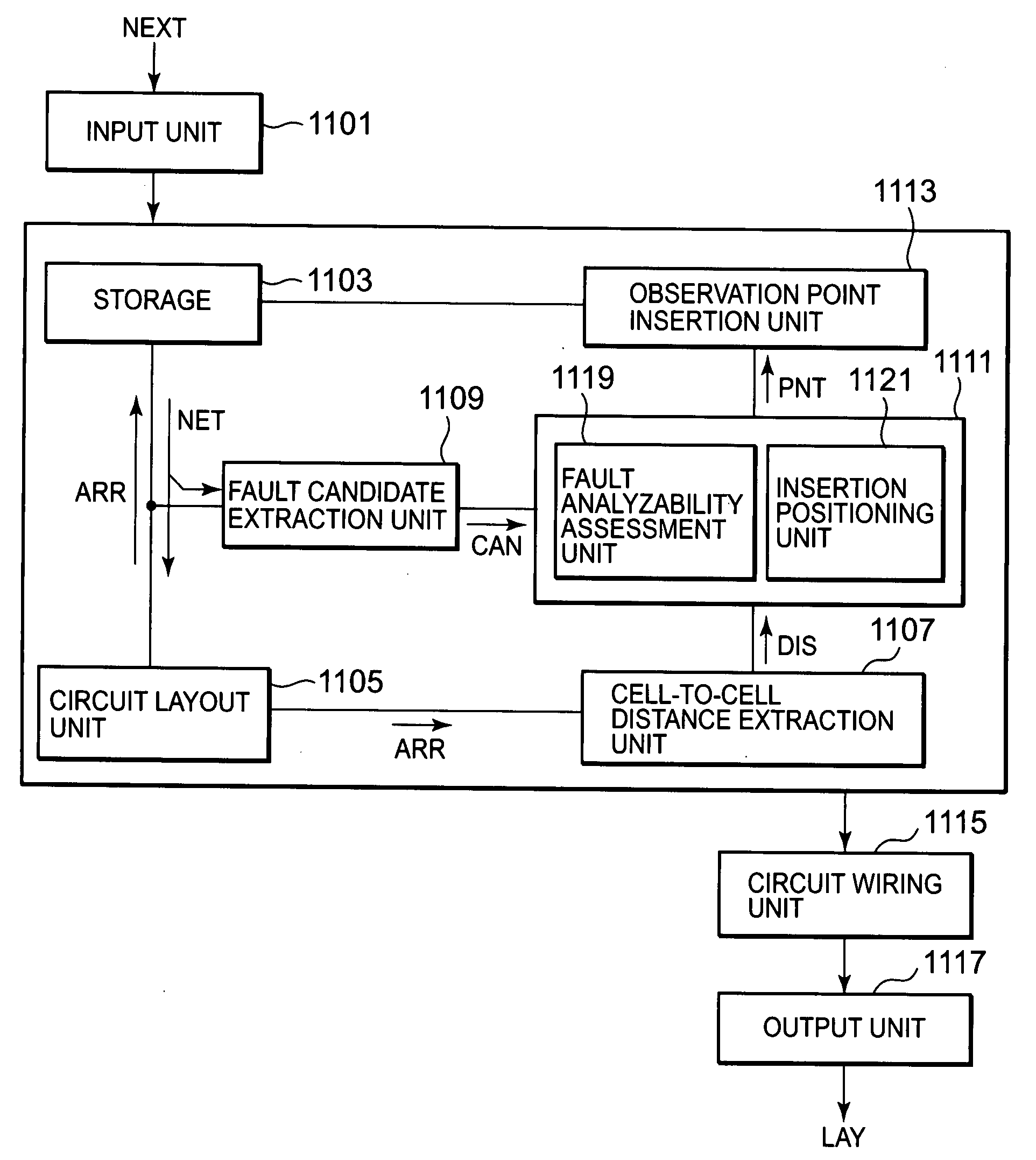
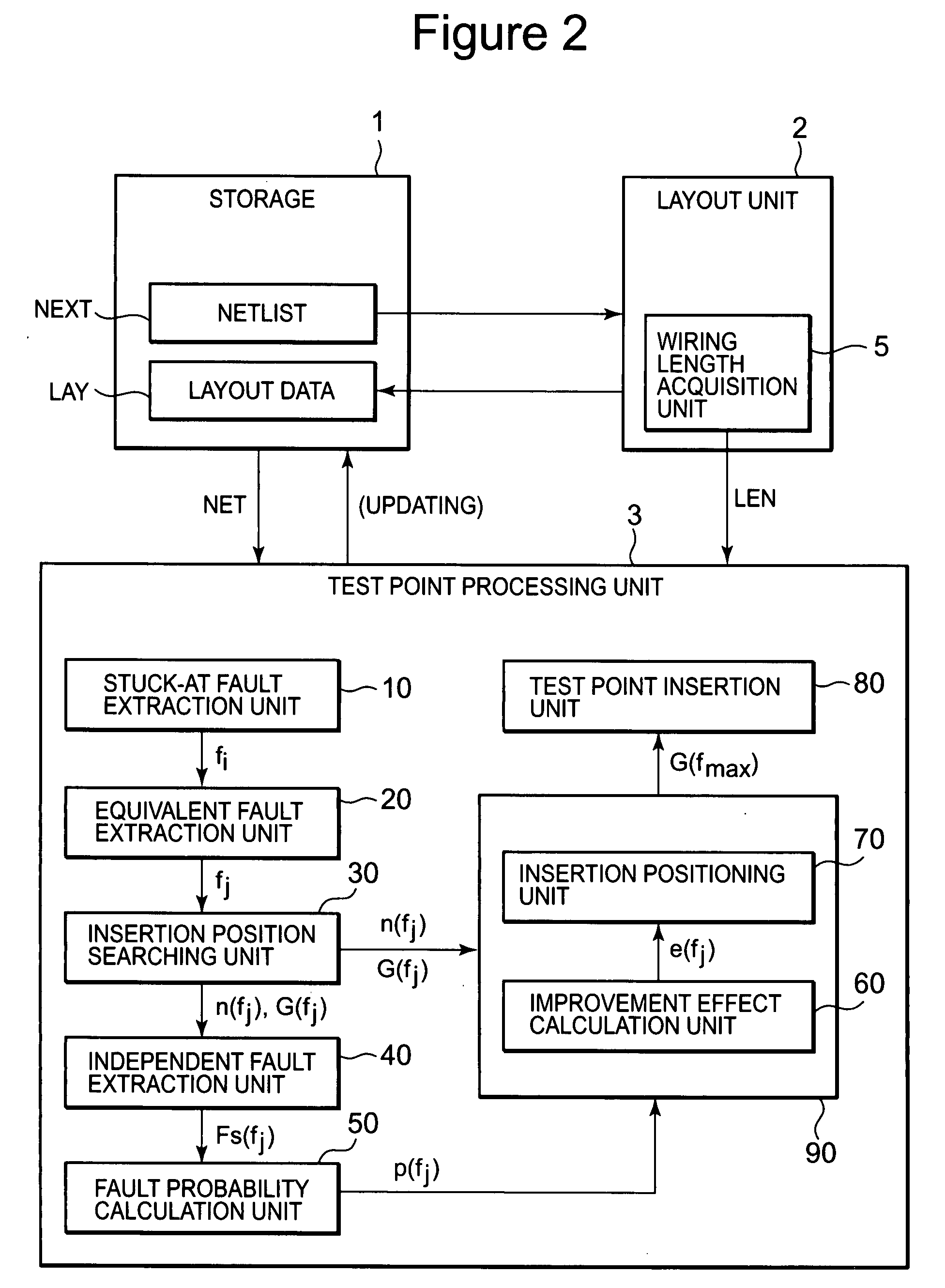
[0064]FIG. 2 is a block diagram illustrating a configuration of a circuit design system related to a first embodiment of the present invention. That circuit design system comprises a storage 1, a layout unit 2 and a test point process unit 3. The netlist NET indicating connection information on the circuit as a design object and layout data LAY indicating the layout thereof are stored in the storage 1. The layout unit 2 carries out the layout process and prepares the layout data LAY from the netlist NET.

[0065]The test point insertion unit 3 carries out a process of test point insertion. The test point insertion is carried out prior to the layout process. Otherwise, the test point insertion can be carried out after the layout data LAY is temporarily prepared. In that case, the layout unit 2 prepares the layout data LAY again after the test point insertion process. That test point processing unit 3 includes a stuck-at fault extraction unit...

second embodiment

[0123]2-1. Configuration

[0124]In the first embodiment, the test points are inserted so that the equivalent faults fj become independent faults. On the other hand, in a second embodiment, the test point is inserted so that the equivalent fault fj becomes an element of the “independent fault pair”. Here, the independent fault pair means a set of equivalent faults being positioned at mutually adjacent nodes and being deprived of the equivalent relation with the other faults. That is, a certain independent fault pair is configured by mutually equivalent two equivalent faults. Those two equivalent faults are positioned at the adjacent node. Accordingly, in the first embodiment, the fault sites are narrowed down to one node. In contrast, in the second embodiment, the fault sites are narrowed down up to two nodes.

[0125]FIG. 14 is a block diagram illustrating a configuration of a circuit design system related to a second embodiment of the present invention. In the present embodiment, like r...

third embodiment

[0142]3-1. Configuration

[0143]FIG. 19 is a block diagram illustrating a configuration of a circuit design system related to a third embodiment of the present invention. In the present embodiment, like reference characters designate the same or similar parts for likewise configurations throughout the figures thereof so that repetitious description will be omitted appropriately.

[0144]According to the present embodiment, compared with the first embodiment, an independent fault extraction unit 40 is omitted. In addition, instead the fault probability calculation unit 50, a fault probability calculation unit 50′ is provided. In the case where a single stuck-at fault has taken place, that fault probability calculation unit 50′ calculates probability of the relevant single stuck-at fault corresponding with the equivalent fault fj. And the calculated probability is used as the above described probability p(fj).

[0145]3-2. Process

[0146]FIG. 20 is a flow chart illustrating the summary of the t...


PUM


Abstract

A circuit design program product to cause a computer to execute a circuit design process based on a test point insertion, includes: a step for making reference to a netlist to extract a plurality of equivalent faults fj; a step for searching a number n(fj) of test point required for a number of the equivalent fault keeping equivalent relation with a search object equivalent fault fj with each of a plurality of equivalent faults as the search object equivalent fault to become a predetermined number and a insertion position G(fj); a step for calculating probability p(fj) of a single stuck-at fault being included in a set of equivalent faults including at least a search object equivalent fault fj at an occasion when the relevant stuck-at fault takes place in the circuit; a step for calculating a parameter e(fj) derived by an equation: e(fj)=p(fj)/n(fj) on each pattern of an insertion position G(fj); and a step for determining the insertion position G(fmax) giving the maximum value among the calculated parameters e(fj) as a position where the test point is inserted.

Description

BACKGROUND OF THE INVENTION[0001]1. Field of the Invention[0002]The present invention relates to design technology on semiconductor integrated circuits. In particular, the present invention relates to a circuit designing system carrying out circuit designing processing based on a Test Point Insertion method and a circuit designing program.[0003]2. Description of Related Art[0004]In the field of semiconductor integrated circuits, there is a possibility of including defective products in the produced products at some percentages.[0005]Accordingly, during the testing step, the defective products are removed and only good products are shipped. A yield rate at the occasion is called a yield factor. In order to improve the yield factor, it is necessary to clarify to improve the manufacturing process.[0006]However, in the recent years, as the microtechnology is applied to semiconductor integrated circuits more, failure analysis is becoming more difficult. A reason thereof is that a failure...

Claims


Application Information

Patent Timeline
Patent Type & Authority Applications(United States)
IPC IPC(8): G06F11/00G06F17/50
CPCG01R31/318357G06F17/505G01R31/318364G06F30/327
Inventor NONAKA, JUNPEI
Owner RENESAS ELECTRONICS CORP
Why Eureka
Try Eureka