

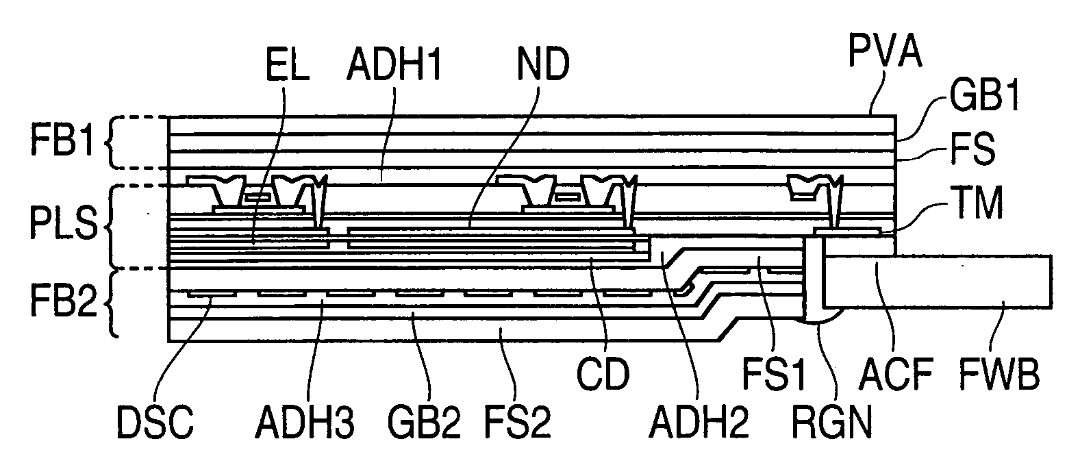
Organic EL display device
a technology of organic el and display device, which is applied in the direction of organic semiconductor device, discharge tube/lamp details, discharge tube luminescnet screen, etc., can solve the problems of easy degradation of desiccant compared to the other members, loss of desiccant function,
- Summary
- Abstract
- Description
- Claims
- Application Information
AI Technical Summary
Benefits of technology
Problems solved by technology
Method used
Image

Examples
Embodiment Construction
[0035] Embodiments of an organic EL display device according to the present invention will be explained hereinafter in conjunction with the drawings.
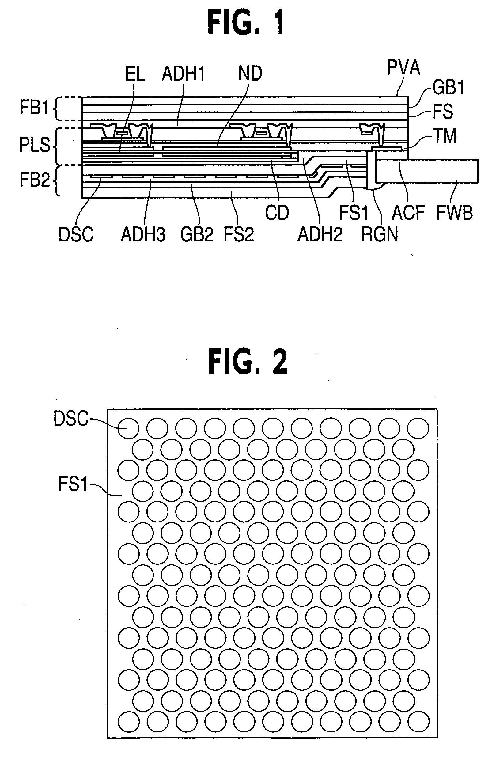
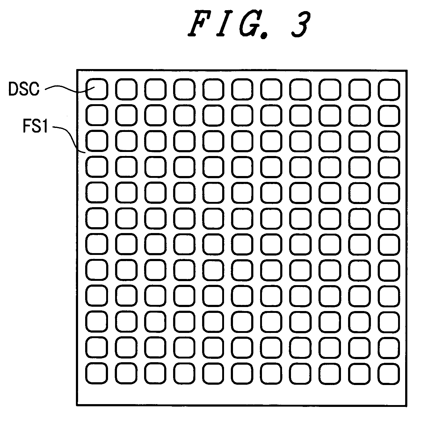
[0036]FIG. 4A and FIG. 4B are diagrams showing one embodiment of the constitution of a pixel of the organic EL display device according to the present invention.
[0037]FIG. 4A is a plan view showing one pixel of the organic EL display device and a portion in the vicinity of the pixel. The respective pixels of the organic EL display device are, for example, formed on a surface of a transparent substrate in a matrix array, and one of the pixels is shown in FIG. 4A. In each pixel, there is a minute circuit which is formed by stacking a conductive layer, a semiconductor layer, an insulation layer and the like, which are formed in given patterns.
[0038] That is, in the drawing, one pixel has an upper side thereof, as shown in FIG. 4A which is defined by a gate signal line GL which selectively drives the pixel, a left side thereof which is d...
PUM
 Abstract
Description
Claims
Application Information