Nitride semiconductor laser device and method of manufacturing the same

a laser device and semiconductor technology, applied in the field of semiconductor laser devices and a manufacturing method of semiconductor laser devices, can solve the problems of difficult growth of active layers containing a large amount, and achieve the effect of avoiding degradation and local segregation

Inactive Publication Date: 2007-05-03
SAMSUNG ELECTRONICS CO LTD
View PDF11 Cites 15 Cited by
  • Summary
  • Abstract
  • Description
  • Claims
  • Application Information

AI Technical Summary

Benefits of technology

[0009] The present invention may provide a nitride semiconductor laser device using an AlxInyGa1-x-yN-based clad layer designed to eliminate degradation and local segregation of an active layer.
[0012] The metal layer and the metal-based clad layer having a ridge shape should be formed of a material with a low optical absorption coefficient K in order to prevent loss of laser light generated in the active layer when being confined. In particular, the metal layer may be formed of a low contact resistance material.

Problems solved by technology

However, the conventional growth technique and structure make it difficult to grow an active layer containing a large amount of In.

Method used


Image

  • Nitride semiconductor laser device and method of manufacturing the same
  • Nitride semiconductor laser device and method of manufacturing the same
  • Nitride semiconductor laser device and method of manufacturing the same

Examples


Embodiment Construction

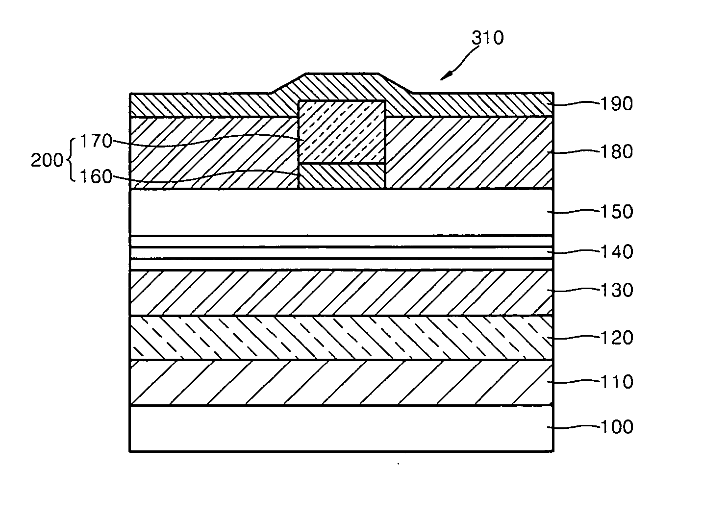
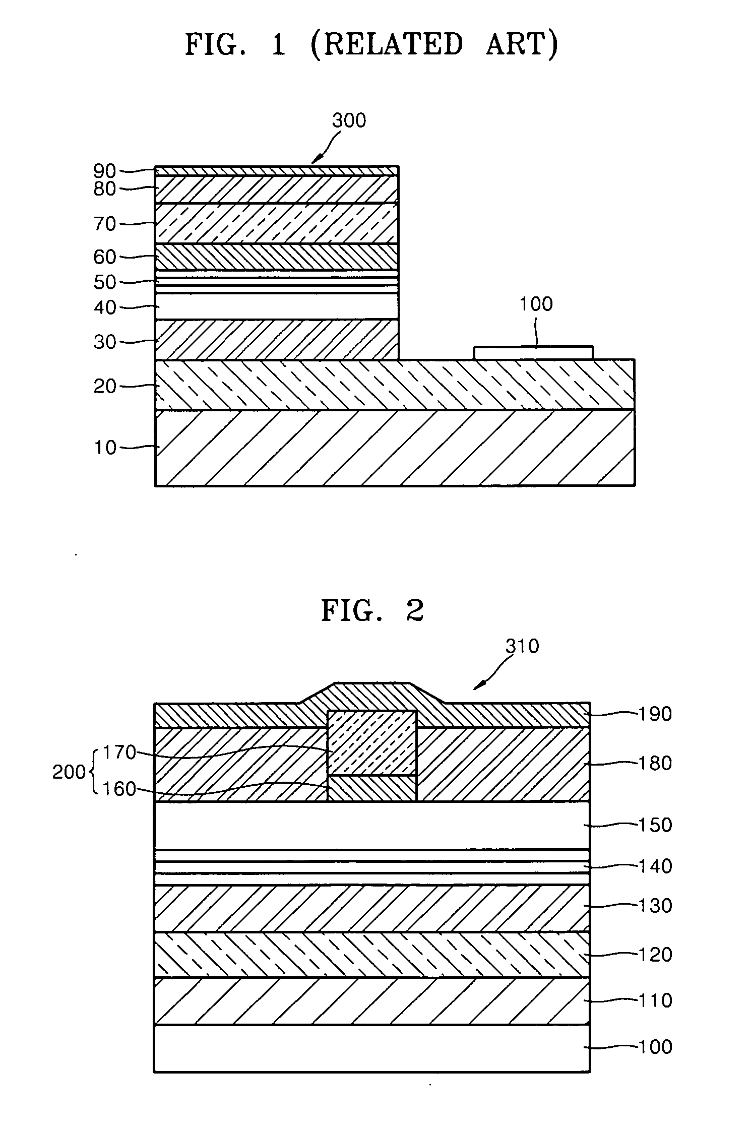
[0033] A semiconductor laser device and method of fabricating the same according to preferred embodiments of the present invention will now be described more fully with reference to the accompanying drawings. The invention may, however, be embodied in many different forms and should not be construed as being limited to the embodiments set forth herein. That is, a semiconductor laser device according to the present invention may have various other stack structures than described herein.

[0034]FIG. 2 is a cross-sectional view of a semiconductor laser device according to an embodiment of the present invention with a metal layer and a metal-based clad layer. Referring to FIG. 2, the semiconductor laser device includes a substrate 100, and an n-material layer 110, an n-clad layer 120, an n-light waveguide layer 130, an active region 140, a nitride semiconductor layer (p-waveguide layer) 150, a metal layer 160 and a metal-based clad layer 170 sequentially formed on the substrate 100. The ...


PUM

PropertyMeasurementUnit
thicknessaaaaaaaaaa
thicknessaaaaaaaaaa
thicknessaaaaaaaaaa

Abstract

A semiconductor laser device is provided. The semiconductor laser device includes a substrate, and an n-material layer, an n-clad layer, an n-light waveguide layer, an active region, a nitride semiconductor layer, a metal layer and a metal-based clad layer sequentially formed on the substrate. The metal layer and the metal-based clad layer have a ridge shape and a current blocking layer is formed on sidewalls of the metal layer and the metal-based clad layer and an exposed surface of the nitride semiconductor layer. A p-electrode layer is formed on the ridge shaped metal layer and the current blocking layer. The semiconductor laser device uses the metal-based clad layer instead of AlxInyGa1-x-yN-based p-clad layer, thus preventing degradation of the active region. The semiconductor laser device also includes the thin metal layer between the metal-based clad layer and a p-GaN material of the nitride semiconductor layer, thus reducing contact resistance therebetween. Thus, it is possible to fabricate a high power, low voltage semiconductor laser device having a visible light wavelength.

Description

CROSS-REFERENCE TO RELATED PATENT APPLICATION [0001] This application claims the benefit of Korean Patent Application No. 10-2005-0105061, filed on Nov. 3, 2005, in the Korean Intellectual Property Office, the disclosure of which is incorporated herein in its entirety by reference. BACKGROUND OF THE DISCLOSURE [0002] 1. Field of the Disclosure [0003] The present disclosure relates to a semiconductor laser device and a method of manufacturing the semiconductor laser device, and more particularly, to a semiconductor laser device using a metal contact layer and a conductive metal-based material as a clad layer instead of an AlGaN-based material and a method of fabricating the same. [0004] 2. Description of the Related Art [0005] A semiconductor laser device using GaN not only is emerging as a promising light source for an optical system for recording and / or reproducing a high-density optical information storage medium such as a blu-ray disc (BD) or a high definition digital versatile d...

Claims


Application Information

Patent Timeline
Patent Type & Authority Applications(United States)
IPC IPC(8): H01S5/00
CPCB82Y20/00H01S5/0425H01S5/20H01S5/2009H01S5/22H01S5/2214H01S5/3214H01S5/3216H01S5/34333H01S5/04253H01S5/04254
Inventor HA, KYOUNG-HORYU, HAN-YOUL
Owner SAMSUNG ELECTRONICS CO LTD
Why Eureka
Try Eureka