Contactor having conductive particles in a hole as a contact electrode

Inactive Publication Date: 2005-05-26
SOCIONEXT INC
View PDF6 Cites 3 Cited by
  • Summary
  • Abstract
  • Description
  • Claims
  • Application Information

AI Technical Summary

Benefits of technology

[0090] According to the present invention, simply having the contactor adjoin the object to be tested can have the contactor contact the object to be tested with s

Problems solved by technology

a) A manufacturing cost of the contactor is high, because the needles are formed one by one.
Thus, it is difficult to manufacture the contactor capable of contacting a plurality of LSI circuits all at once.
Also, because the contact electrode is a metal bump, the contact electrode lacks flexibility.
b) Since the bump as a contact electrode is generally formed by laminating metal plating layers, manufacturing the bump takes a long time and the bump cost is high.
b) Since it is difficult to embed the conductive materials with a fine pitch into the rubber, the contactor using an anisotropic conductive rubber cannot be used to test an LSI circuit having terminals with a fine pitch.
Thus, the above-mentioned contactors commonly have the following problems.
With the conventional contactors, because of the different heights of the electrodes and other reasons, it is diffi

Method used


Image

  • Contactor having conductive particles in a hole as a contact electrode
  • Contactor having conductive particles in a hole as a contact electrode
  • Contactor having conductive particles in a hole as a contact electrode

Examples


Example

EXAMPLE 1

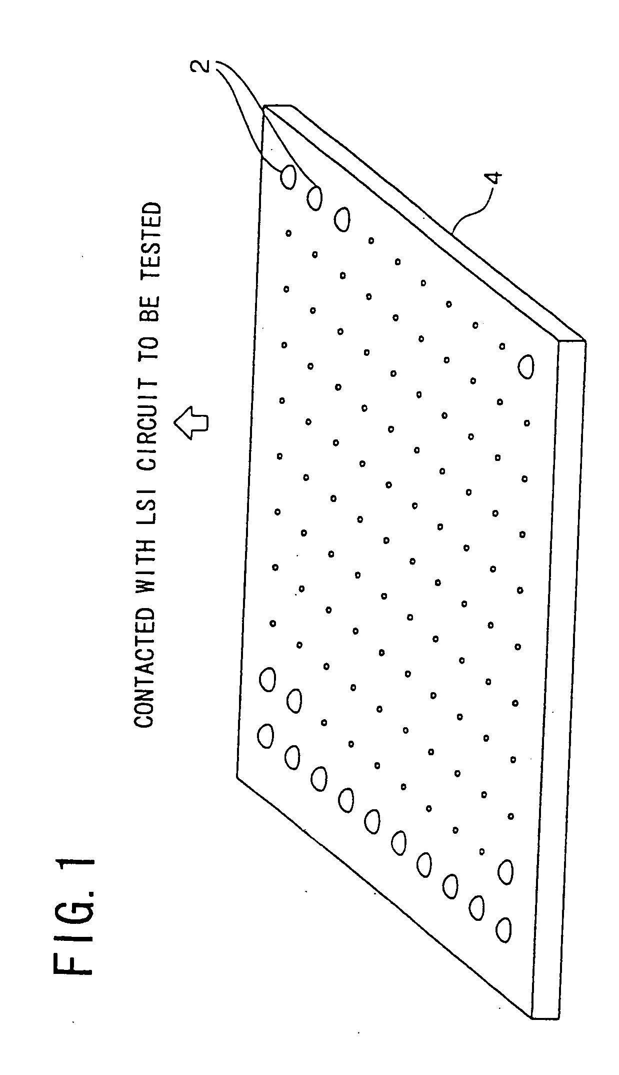
[0204] The contactor according to the present embodiment was used as a contactor for a CSP (LGA type) in the form of a wafer. The CSP had pad terminals (electrodes) with a 500-μm pitch. Each of LSI circuits to be tested was a 10-mm-square LSI chip and had 360 terminals in a full matrix. The LSI chip had been formed in an 8-inch wafer. The wafer had approximately 250 LSI chips and 90,000 terminals in total.

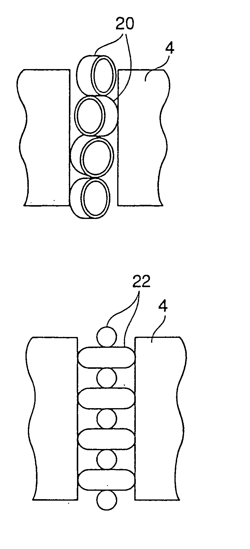
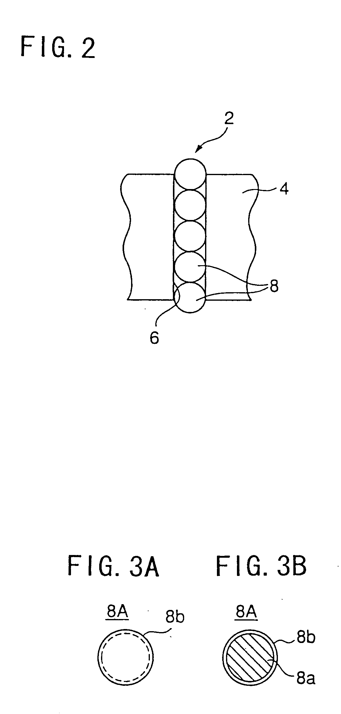
[0205] A 500-μm-thick silicon wafer was used as the insulating substrate 70 of the contactor. The through holes 72, each having a diameter of 150 μm, were formed in this silicon wafer with a 500-μm pitch by a photo-excited electrolytic grinding method. The terminal 76 for circuit wiring was formed on one end of each of the through holes 72. The counterbore 72a was formed on the other end. Each of the through holes 72 was filled with the above-mentioned conductor by a liquid suction method.

[0206] The above-mentioned CSP in the form of a wafer was brought closer to the co...

Example

EXAMPLE 2

[0208] A contactor for testing the same CSP in the form of a wafer as the above-mentioned Example 1 was formed using SN-58Bi, which is a low-melting-point solder, as the conductor.

[0209] First, registration was performed between the contactor and the LSI chips in the wafer at a normal temperature. Thereafter, the contactor and the wafer were heated to 125° C. so that the conductors became semi-molten. Then, the bump portions of the conductors were bonded to the terminals of the LSI chips with a load of 1 g a terminal by thermo-compression bonding, successfully with an excellent contact.

[0210] In the present example, after the bump portions of the conductors were bonded to the terminals of the LSI chips, the contactor and the wafer were mounted on a prober, which was a test device. Then, the prober was connected to the terminals for circuit wiring formed on the insulating substrate of the contactor so as to carry out a functional test. Further, after the functional test, ...

Example

EXAMPLE 3

[0212] A contactor having the same structure as the above-mentioned Example 1, except for a low-melting-point solder used as the conductor, was prepared. After the contactor was heated to 150° C. so that the solder became molten, the contactor was brought into contact with the wafer with a load of zero. This contact was performed in a nitrogen atmosphere to avoid forming an oxide film on a surface of the solder. Then, a temperature cycling test was carried out at temperatures from −25° C. to 125° C., providing the same result as a conventional method.


PUM


Abstract

A contactor is provided which contactor comprises an insulating substrate, a concave portion formed in the insulating substrate and extending in a perpendicular direction from a surface thereof, and elastic conductive particles disposed in the concave portion. A part of one of the conductive particles protrudes from the surface of the insulating substrate.

Description

BACKGROUND OF THE INVENTION [0001] 1. Field of the Invention [0002] The present invention generally relates to a contactor for electronic parts and, more particularly, to a contactor for electronic parts which contactor provides electrical conduction by contacting an electrode of a semiconductor device, such as an LSI circuit, to test the semiconductor device, and to a testing method using such a contactor. [0003] Recently, a manufacturing technology of a semiconductor substrate and the like has been remarkably developed. Accordingly, a wiring pattern of a semiconductor device, such as an LSI circuit, has become finer, and terminals have been remarkably increased in number and miniaturized. [0004] Also, miniaturization and high-density packaging are required for an electronic device using the semiconductor devices. For example, production and sales of mobile devices, such as a cellular phone, a mobile PC and a video camera, which are required to be small and of high performance are ...

Claims


Application Information

Patent Timeline
IPC IPC(8): G01R31/26G01R1/04G01R1/067G01R1/073H01L21/66H01L23/498
CPCG01R1/0483G01R1/06711G01R1/06733G01R1/06755G01R1/07314H01L2924/0002H01L23/49827H01L2924/00G01R1/067
Inventor MARUYAMA, SHIGEYUKIKIDA, SUSUMUWATANABE, NAOYUKIHASHITANI, TAKAFUMIYANO, EIMIDORIKAWA, ICHIRO
Owner SOCIONEXT INC
Why Eureka
Try Eureka