Resistive type touch panel

a type and touch panel technology, applied in the field of resistive type touch panel, can solve problems such as errors in detecting pen touch points, and achieve the effect of reducing the magnitude of minimizing the generation of erroneous coordinate information, and reducing the deformation of the substra

Inactive Publication Date: 2005-05-26
LG DISPLAY CO LTD
View PDF8 Cites 50 Cited by
  • Summary
  • Abstract
  • Description
  • Claims
  • Application Information

AI Technical Summary

Benefits of technology

[0032] The spacers are designed and positioned between the first and second substrates to avoid inadvertent contact between the first and second conductive layers when the first substrate is deformed during operational use of the touch screen. During operation, touching the display screen with an activation force may cause deformation of the first substrate resulting in contact between first and second conductive layers. Contact between the first and second conductive layers results in the generation of coordinates indicative of the location that the display screen was touched. By minimizing inadvertent contact, generation of erroneous coordinate information can be minimized.
[0033] Distinguishing the difference between a desired touch and an inadvertent touch may be realized using the spacer

Problems solved by technology

As a result, the touch panel controller 30 and the system 40 utilize the middle point and thereby generate an error in detecting the pen touch point (T1).
During operat

Method used


Image

  • Resistive type touch panel
  • Resistive type touch panel
  • Resistive type touch panel

Examples


first embodiment

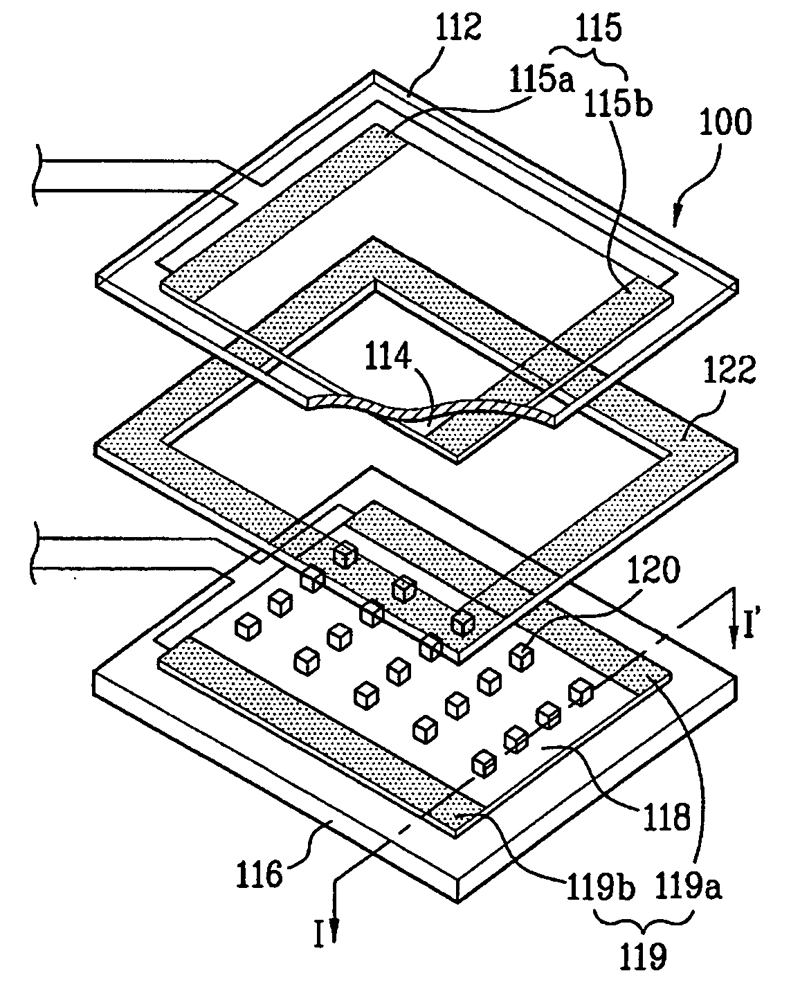
[0059]FIG. 7 is a cross sectional view along I-I′ of a portion of the resistive type touch panel illustrated in FIG. 6 depicting a first embodiment. In FIG. 7, spacers 120 are disposed on an upper substrate 112 or a lower substrate 116. The spacers 120 may be formed by printing or photo process. The spacers 120 may be disposed on an area of the touch panel with a predetermined center-to-center distance (Lp) between the spacers 120 such as between about 0.5 mm and 0.6 mm. As used herein, the term “about” should be construed to be plus and minus 10% of the measure value, or plus and minus 5% of the measured value unless otherwise indicated.

[0060] Each spacer 120 has a predetermined length (Ld) and a predetermined width. The width and the length may be substantially equal, such as between about 40 μm and 50 μm. In addition, each of the spacers 120 may have a predetermined height, such as between about 5 μm and 13 μm. Accordingly, the area of the first and second surface of each of the...

second embodiment

[0068]FIG. 9 is a cross sectional view along I-I′ of a portion of the resistive type touch panel 100 illustrated in FIG. 6. In FIG. 9, spacers 120 are formed on an area of the lower substrate 116. In addition, the lower substrate 116 includes a plurality of edge spacers 125 disposed adjacent to an X-electrode bar 115 or a Y-electrode bar 119, and adjacent to a periphery of the conductive layers 116 and 118.

[0069] The edge spacers 125 are formed to have a hemispherical surface. The hemispherical surface is formed to be in contact with one of the transparent conductive layers 116 and 118 when an activation force is applied. Absent an activation force, the hemispherical surface is positioned proximate one of the transparent conductive layers 116 and 118 with a space there between. With the exception of the edge spacers 125, the resistive type touch panel according to the second embodiment has a similar structure to the resistive type touch panel discussed with reference to FIGS. 6-8. ...

third embodiment

[0071]FIG. 10 is a plan view of a portion of a resistive type touch panel 100 showing a disposition of spacers according to the third embodiment. In the resistive type touch panel 100 shown in FIG. 10, a plurality of spacers 130 may be formed in polygonal column shape, such as a hexahedral shape. Accordingly, the spacers 130 may each have a substantially similar length (Ld) and width that is between about 40 μm and 50 μm, and a height of between about 5 μm and 13 μm.

[0072] The spacers 130 may be disposed on one of the first substrate and the second substrate as previously discussed. In addition, the spacers 130 may be distributed in a predetermined pattern so that the spacers 130 are staggered with respect to each other. Accordingly, portions of the predetermined pattern may be configured to resemble a diamond shape (a-b-c-d) as illustrated.

[0073] In FIG. 10, the spacers 130 can be grouped into groups of spacers forming a plurality of horizontal lines along a first axis. In a firs...


PUM


Abstract

A resistive type touch panel includes a first substrate aligned to be facing a second substrate. The first substrate includes a first conductive layer and the second substrate includes a second conductive layer. A plurality of spacers each having a polygonal column shape are disposed between the first and second substrates in predetermined positions. The geometry and center-to-center spacing of the spacers minimizes detection of a distributed activation force applied to one of the first and second substrate while still providing sensitivity to detect concentrated application of an activation force to one of the first and second substrates.

Description

PRIORITY CLAIM [0001] This application claims the benefit of the Korean Application No. P2003-83690 filed on Nov. 24, 2003, which is hereby incorporated by reference. BACKGROUND [0002] 1. Technical Field [0003] The present invention relates to a touch panel, and more particularly, to a resistive type touch panel that is configured to distinguish between inadvertent contact with the touch panel and desired selection of a displayed item. [0004] 2. Related Art [0005] Touch panels are widely integrated with display surfaces of display devices such as electronic calculators, liquid crystal display (LCD) devices, plasma display panel (PDP) devices, electroluminescence (EL) devices, and cathode ray tubes (CRTs). Touch panels may be classified into an analog resistive type, a capacitive type, and an EM (Electro-magnetic) type. In general, touch panels are capable of sensing the location on the display surface where a user contacts the display surface with an object such as a pen, a finger, ...

Claims


Application Information

Patent Timeline
IPC IPC(8): G02F1/1339G06F3/045G09G5/00
CPCG06F3/045G02F1/1339
Inventor KONG, NAM YONGYOU, TAE HOPARK, HEE JEONG
Owner LG DISPLAY CO LTD
Why Eureka
Try Eureka