Chemical mechanical polish process control method using thermal imaging of polishing pad

a technology of thermal imaging and mechanical polishing, applied in the direction of grinding machine components, basic electric elements, electric instruments, etc., can solve the problems of difficult lithographic image and pattern layer application to rough surfaces

Inactive Publication Date: 2005-06-02
IND TECH RES INST
View PDF13 Cites 31 Cited by
  • Summary
  • Abstract
  • Description
  • Claims
  • Application Information

AI Technical Summary

Benefits of technology

[0015] It is a general object of the present invention to provide an improved method of monitoring and controlling CMP processes.

Problems solved by technology

It is desirable that insulating layers have smooth topography because it is difficult to lithographically image and pattern layers applied to rough surfaces.
An important challenge in CMP is to determine the process endpoint in real time without a necessity for interrupting the CMP process, removing the substrate from the polishing apparatus, and physically examining the substrate surface by techniques which ascertain film thickness and / or surface topography.
Another challenge in CMP processes is real time process control, whereby on-line, in real time CMP process parameters are adjusted in order to improve polish removal rate uniformity.

Method used


Image

  • Chemical mechanical polish process control method using thermal imaging of polishing pad
  • Chemical mechanical polish process control method using thermal imaging of polishing pad
  • Chemical mechanical polish process control method using thermal imaging of polishing pad

Examples


Embodiment Construction

[0032] The improved method of controlling a CMP (Chemical Mechanical Polishing) process for a semiconductor substrate being polished by a rotating polishing pad will now described in detail.

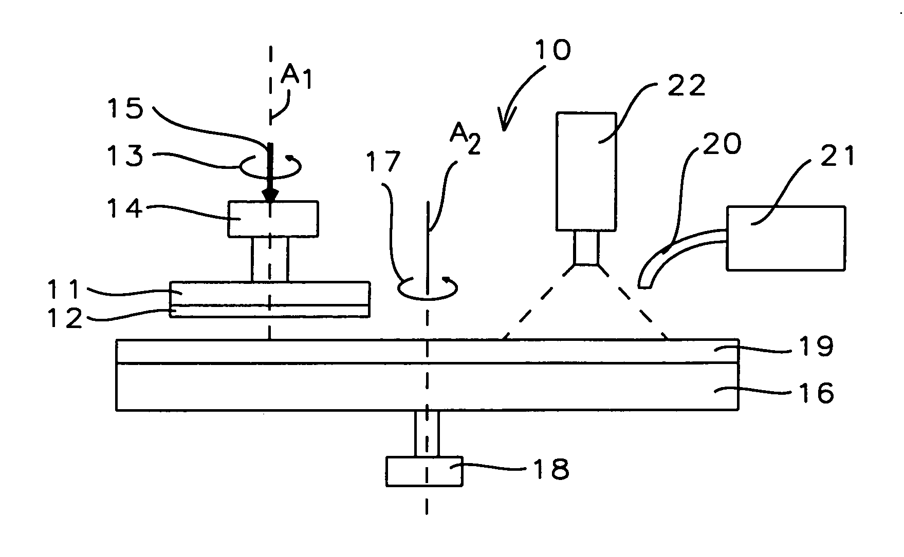
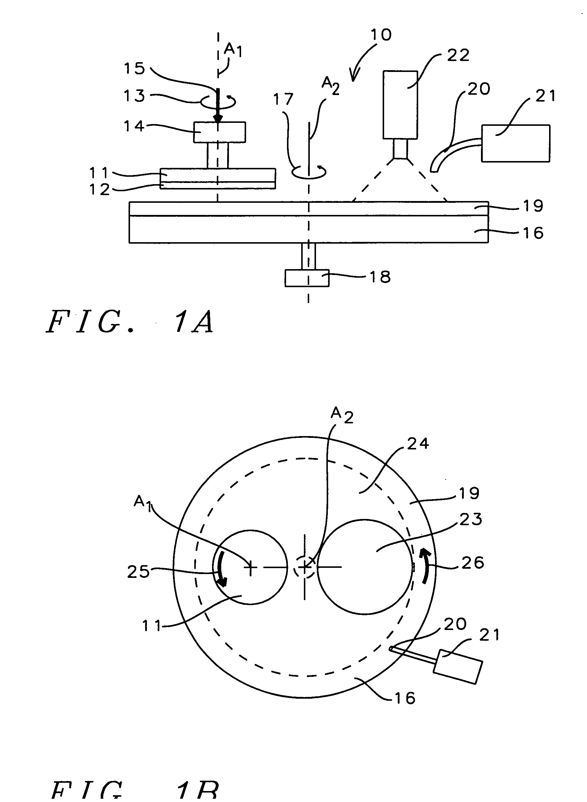
[0033]FIGS. 1A and 1B are schematic views of a CMP (Chemical Mechanical Polishing) apparatus for use in accordance with the method of the invention. In FIG. 1A, the CMP apparatus, generally designated as 10, is shown schematically in cross-sectional representation. The CMP apparatus 10 includes a substrate carrier 11 for holding a semiconductor substrate 12. The substrate carrier 11 is mounted for continuous rotation about axis A1 in a direction indicated by arrow 13 by drive motor 14. The substrate carrier 11 is adapted so that a force indicated by arrow 15 is exerted on semi-conductor substrate 12. The CMP apparatus 10, also, includes a polishing platen 16 mounted for continuous rotation about axis A2 in a direction indicated by arrow 17 by drive motor 18. A polishing pad 19 formed of a materi...


PUM


Abstract

A method and apparatus for controlling CMP (Chemical Mechanical Polishing) for semiconductor substrates includes an infrared camera for detecting and mapping in two dimensions the thermal image of the polishing pad during CMP. The thermal image of the polishing pad is then analyzed and used to control the process parameters of the CMP process. Analysis of the thermal image of the polishing pad allows real time endpoint detection of the CMP process and, also, real time adjustment of process parameters to improve the uniformity of removal of material across the semiconductor substrate.

Description

BACKGROUND OF THE INVENTION [0001] (1) Field of the Invention [0002] This invention relates to a method and apparatus for controlling a CMP (Chemical Mechanical Polishing) process in real time by measuring and mapping in two dimensions the surface temperature of the polishing pad during the CMP process. Additionally, the invention is directed to a method of determining the uniformity of removal of material from a semiconductor substrate during chemical mechanical polishing of the semiconductor substrate. [0003] (2) Description of Related Art [0004] In the fabrication of semiconductor integrated circuits CMP (Chemical Mechanical Polishing) can be used to remove different layers of material from the surface of a semi-conductor substrate. For example, following contact hole formation in an insulating layer, a metallization layer is deposited and then CMP is used to produce planar metal plugs embedded in the insulating layer. Similarly, interconnection wiring can be formed by first etch...

Claims


Application Information

Patent Timeline
Patent Type & Authority Applications(United States)
IPC IPC(8): B24B37/04B24B49/12B24B49/14H01L21/3105H01L21/321H01L21/324
CPCB24B37/015H01L21/3212H01L21/31053B24B49/12
Inventor CHEN, LAI-JUH
Owner IND TECH RES INST
Why Eureka
Try Eureka