
Method and circuit for compensating for tunneling current

a tunneling leakage current and tunneling current technology, applied in the field of integrated circuits, can solve the problems of tunneling leakage becoming an appreciable fraction of the total integrated circuit power consumption, affecting the performance and power consumption and affecting the operation of the gate dielectric (often an oxide) thickness

Inactive Publication Date: 2005-06-09
GLOBALFOUNDRIES INC
View PDF11 Cites 4 Cited by
  • Summary
  • Abstract
  • Description
  • Claims
  • Application Information

AI Technical Summary

Problems solved by technology

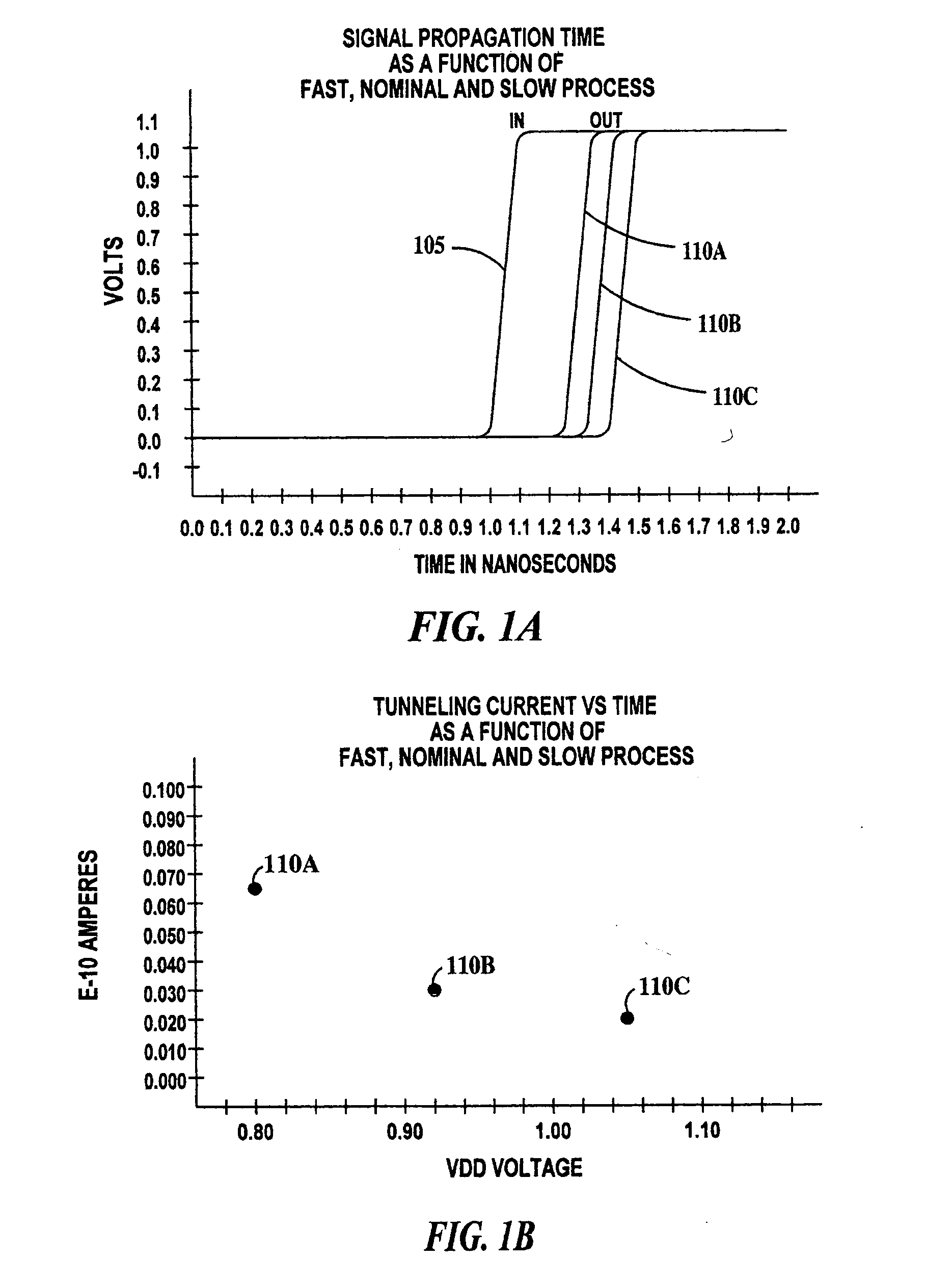
For example, variations in gate dielectric (often an oxide) thickness, FET channel length and threshold voltage will produce skews in performance and in power consumption creating distributions referred to as fast, nominal and slow process, or alternatively as best-case, nominal and worst-case product corners.
Further, as dielectric thicknesses have decreased, tunneling leakage has become an appreciable fraction of the total integrated circuit power consumption.
Tunneling leakage is especially problematic for the best-case or fast process distribution, because the faster devices draw more current than slow devices.
Device dielectric tunneling leakage current can also affect burn-in of integrated circuits.
At these higher burn-in voltages power dissipation of the integrated circuit can be high enough to cause catastrophic failure of both the integrated circuit and the associated burn-in boards and other equipment.

Method used


Image

  • Method and circuit for compensating for tunneling current
  • Method and circuit for compensating for tunneling current
  • Method and circuit for compensating for tunneling current

Examples


Embodiment Construction

[0015] For the purposes of the present invention, tunneling leakage is defined as both the current flow due to a statistical probability that carriers will pass through a dielectric layer having a voltage applied across the dielectric layer and the current flow through a dielectric layer related to dielectric structure and dielectric faults. A gate capacitor is defined as a capacitor formed from a gate, a gate dielectric and the channel region of an NFET or a PFET and commonly referred to as an NCAP or a PCAP respectively. This definition of a gate capacitor is intended to cover all thin dielectric capacitors formed using a thin dielectric film formed on a semiconductor substrate, wherein the semiconductor substrate is one of the plates of the capacitor.

[0016] A fast process or best-case process is defined as a process resulting in an integrated circuit chip having the minimum gate dielectric thickness, shortest channel length and lowest threshold voltage allowed by the manufacturi...


PUM


Abstract

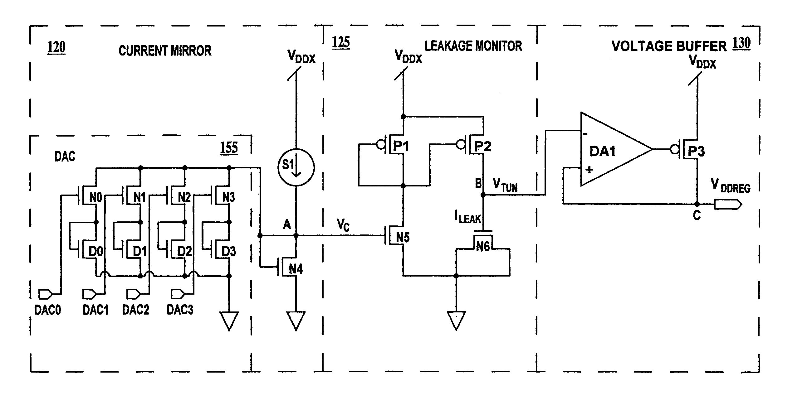
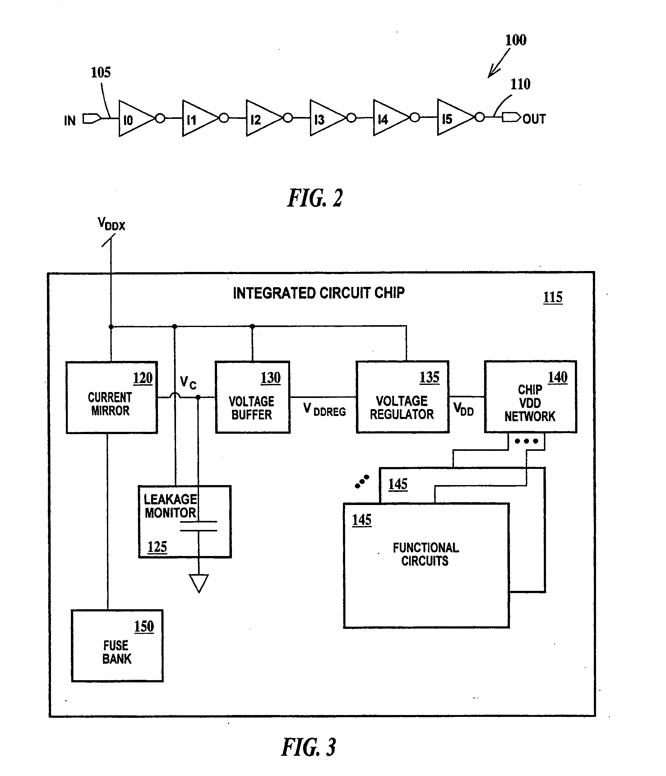
A method and circuit for tunneling leakage current compensation, the method including: forcing a current of known value through a tunneling current leakage monitor device to provide a voltage signal; and regulating an on-chip power supply of the integrated circuit chip based on the voltage signal.

Description

FIELD OF THE INVENTION [0001] The present invention relates to the field of integrated circuits; more specifically, it relates to a circuit and method for compensating for tunneling leakage currents in an integrated circuit chip. BACKGROUND OF THE INVENTION [0002] Integrated circuit manufacturing tolerances on critical field effect (FET) device parameters can affect device performance. For example, variations in gate dielectric (often an oxide) thickness, FET channel length and threshold voltage will produce skews in performance and in power consumption creating distributions referred to as fast, nominal and slow process, or alternatively as best-case, nominal and worst-case product corners. [0003] Further, as dielectric thicknesses have decreased, tunneling leakage has become an appreciable fraction of the total integrated circuit power consumption. Tunneling leakage is especially problematic for the best-case or fast process distribution, because the faster devices draw more curre...

Claims


Application Information

Patent Timeline
IPC IPC(8): G05F3/02G05F3/24
CPCG05F3/242
Inventor ABADEER, WAGDI W.APPLEYARD, JENNIFER E.FIFIELD, JOHN A.TONTI, WILLIAM R.
Owner GLOBALFOUNDRIES INC
Learn More