Power source circuit for high frequency power amplifying circuit and semiconductor integrated circuit for power source and electronics component for power source

a technology power source circuit, which is applied in the direction of amplifiers with semiconductor devices only, amplifiers with semiconductor devices/discharge tubes, amplifiers, etc., can solve the problems of tens of microseconds or longer voltage drop, and the power source voltage of high frequency power amplifying circuit cannot be changed promptly, so as to reduce the size and weight of portable telephones, the effect of large capacity

Inactive Publication Date: 2005-06-09
RENESAS TECH CORP
View PDF1 Cites 106 Cited by
  • Summary
  • Abstract
  • Description
  • Claims
  • Application Information

AI Technical Summary

Benefits of technology

[0006] However, it is expected that the allowance time since the start signal is supplied to the high frequency power amplifying circuit until a high frequency sound signal and data signal are transmitted is shortened to one fraction of a few portion of the allowance time of the narrow-band CDMA in order to enhance the function. Therefore, the power source voltage of the high frequency power amplifying circuit has to be generated in short time but may not be generated in time by using a normal switching regulator.
[0021] Further, according to the invention, operation voltage can be supplied from a common power source circuit and it is unnecessary to provide a smoothing capacitor of large capacity. Therefore, the power source circuit for a high frequency power amplifying circuit, which can contribute to reduction in size and weight of a portable telephone can be realized.

Problems solved by technology

Therefore, the power source voltage of the high frequency power amplifying circuit has to be generated in short time but may not be generated in time by using a normal switching regulator.
However, it takes for a normal switching regulator time of 50 microseconds or longer to increase the output voltage to the original level as described above, so that the power source voltage of the high frequency power amplifying circuit cannot change promptly in response to the start signal and a drop of the voltage for tens of microseconds or longer occurs.

Method used


Image

  • Power source circuit for high frequency power amplifying circuit and semiconductor integrated circuit for power source and electronics component for power source
  • Power source circuit for high frequency power amplifying circuit and semiconductor integrated circuit for power source and electronics component for power source
  • Power source circuit for high frequency power amplifying circuit and semiconductor integrated circuit for power source and electronics component for power source

Examples


first embodiment

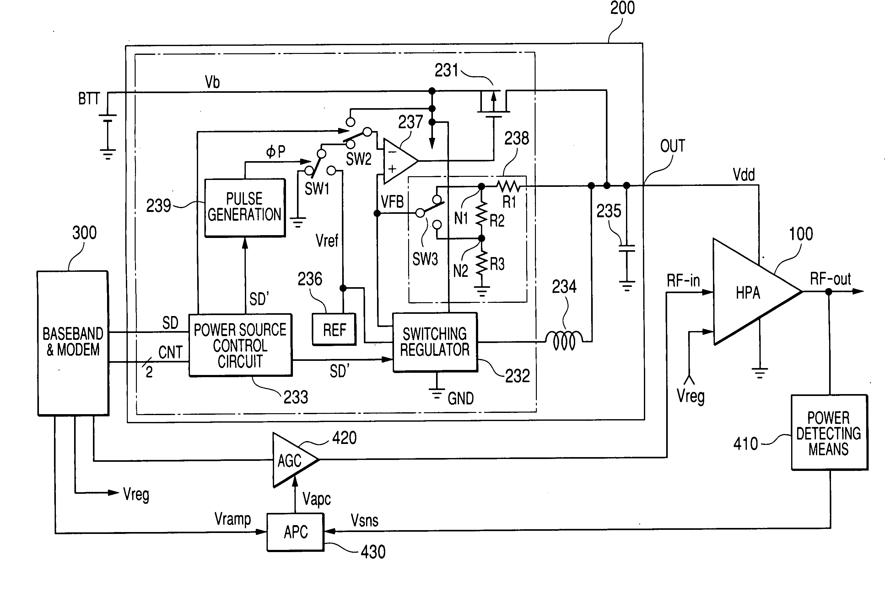
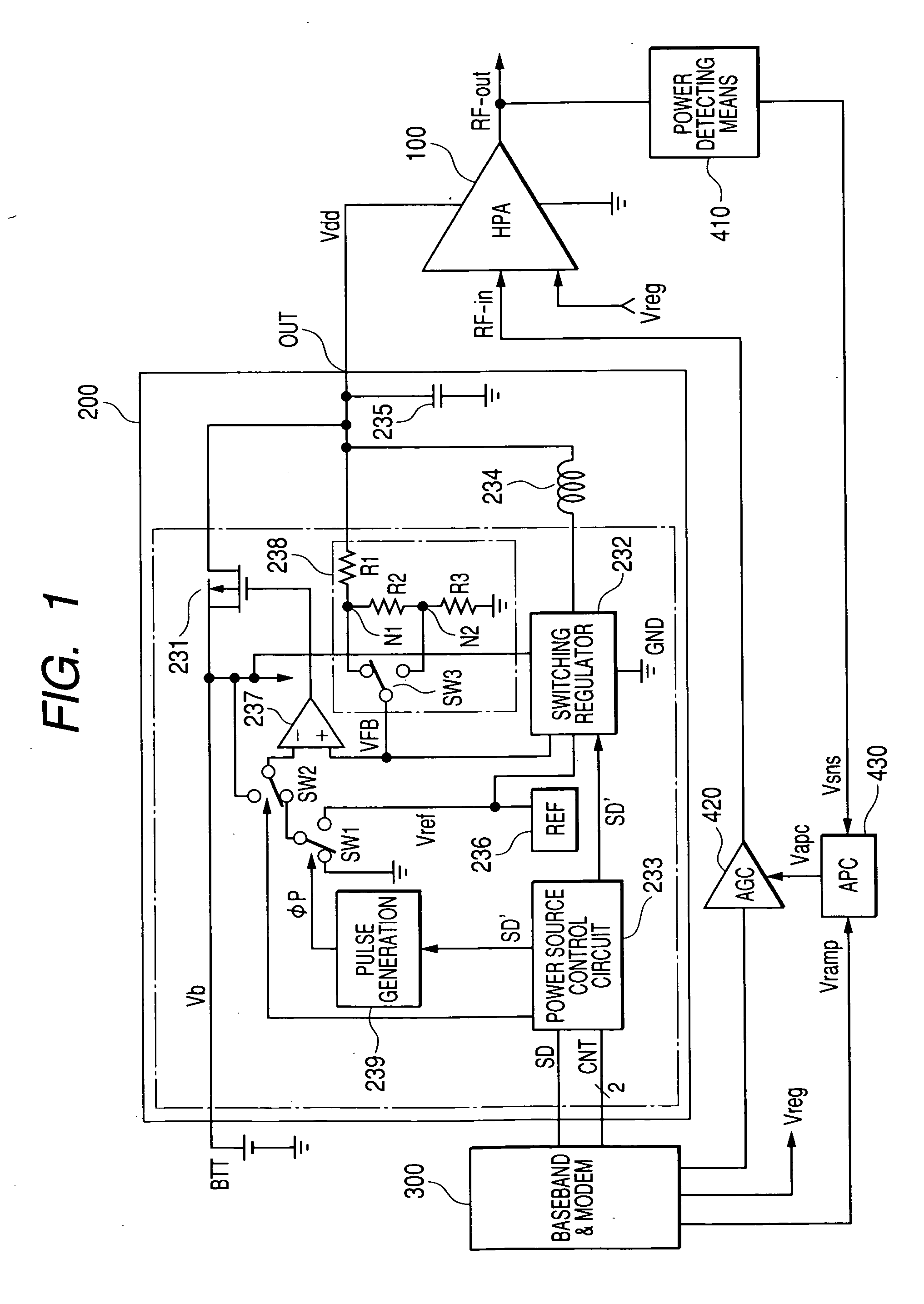
[0034]FIG. 1 shows an embodiment of a power source circuit and a system in the case where the invention is applied to a power source circuit for a high frequency power amplifying circuit of a portable telephone capable of transmitting / receiving data in two systems of the GSM and the CDMA system. FIG. 1 shows an example of the configuration of the CDMA system. The system configuration of the GSM will be described later.

[0035] Shown in FIG. 1 are a high frequency power amplifying circuit 100 for amplifying a transmission signal and outputting the amplified signal; a power source circuit 200 for generating a power source voltage Vdd of the high frequency power amplifying circuit 100 on the basis of a power source voltage Vb from a battery BTT; and a baseband & modem 300 constructed by a baseband circuit for converting a sound signal to a baseband signal, converting a reception signal to a sound signal, and generating a transmission / reception switching signal and a modulating system or...

second embodiment

[0048]FIG. 3 shows an example of a power source circuit and a GSM system of the case where the invention is applied to a power source circuit for the high frequency power amplifying circuit of a portable telephone capable of performing transmission / reception by two systems of the GSM and CDMA. Since the configuration of the power source circuit 200 is the same as that of FIG. 1, its description will not be repeated. In FIG. 3, the same reference numerals are designated to circuits having the same functions as those of FIG. 1 and the description will not be repeated.

[0049] As shown in FIG. 3, in the GSM system, a control voltage Vabc obtained by comparing the output level instruction signal Ramp from the baseband & modem 300 with a detection signal Vsns detected by the power detecting means 410 and outputting a voltage according to the potential difference from the automatic power control circuit (APC) 430 is supplied to the high frequency power amplifying circuit 100 and gain contr...

third embodiment

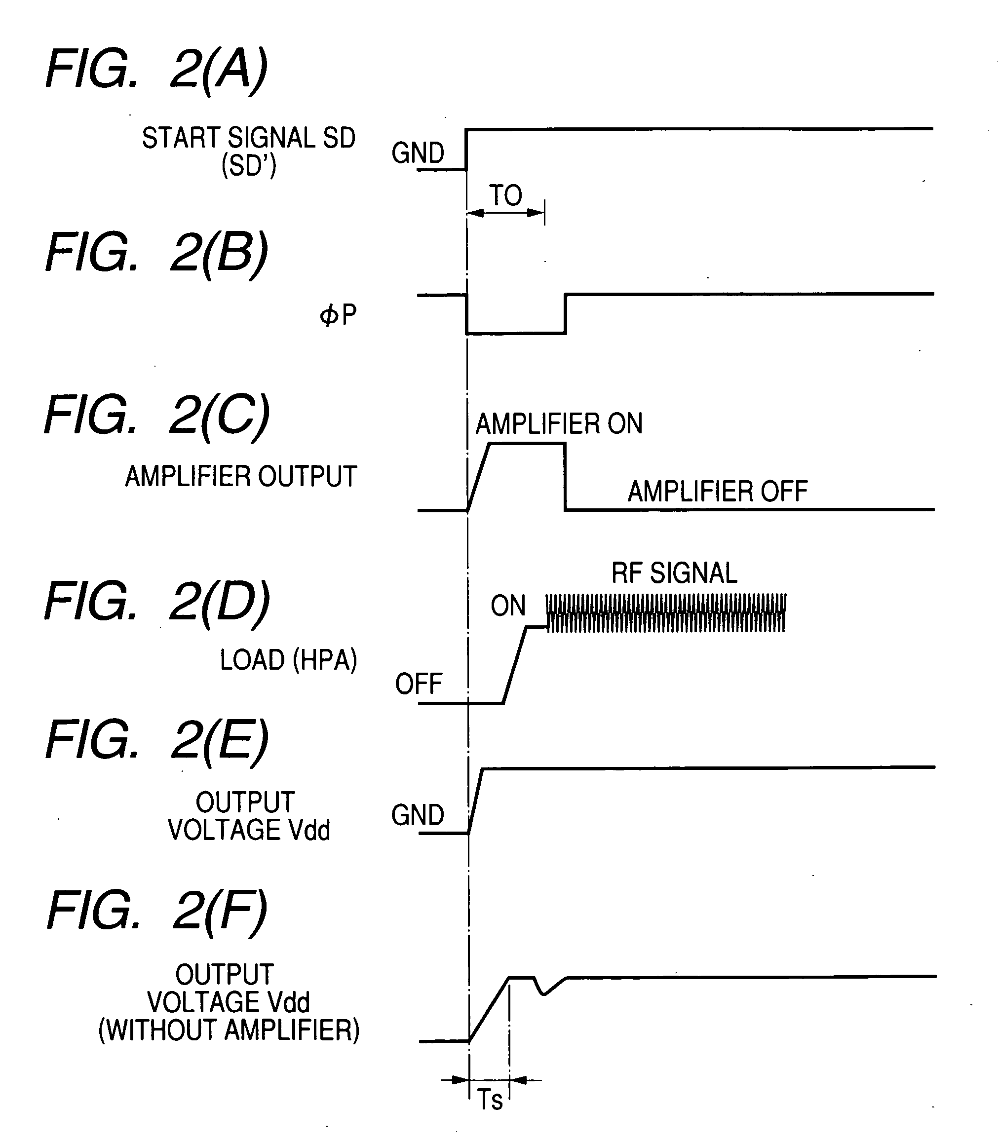
[0057]FIG. 5 shows another embodiment of the power source circuit for a high frequency power amplifying circuit of the invention. The configuration of the power source circuit 200 of the embodiment is almost the same as that shown in FIG. 1 except that a MOSFET TR1 for discharge is added between the voltage output terminal of the power source circuit 200 and the ground point and a MOSFET TR2 is added between the MOSFET TR1 and the ground point so that the output power source voltage Vdd can be decreased to a predetermined set potential at high speed when the MOSFET 231 for voltage control is turned off.

[0058] In the third embodiment, the MOSFET TR1 for discharge is an N-channel MOSFET and operates complementarily to the P-channel MOSFET 2.31 for voltage control in accordance with an output of the amplifier 237. As shown in FIG. 6, the MOSFET TR1 is controlled to turn on only for a period AT in which the MOSFET TR2 is turned off by a signal / φp obtained by inverting the pulse signal ...


PUM


Abstract

The invention realizes a power source circuit for a high frequency power amplifying circuit, which achieves excellent responsiveness of output voltage, can be used for a portable telephone of the GSM or WCDMA and a portable telephone capable of performing communications in two or more communication systems such as the GSM and CDMA and, moreover, has high power efficiency. A power source circuit for a high frequency power amplifying circuit is constructed by using both a first direct current power source circuit such as a series regulator whose power efficiency is not high but which becomes the high level quickly, and a second direct current power source circuit such as a switching regulator, which does not become the high level quickly but whose power efficiency is high. When the power source voltage has to become the high level at high speed, both of the series regulator and the switching regulator are simultaneously operated. When the output power source voltage reaches a predetermined level, the operation of the series regulator is stopped.

Description

CROSS-REFERENCE TO RELATED APPLICATION [0001] The present application claims priority from Japanese patent application No. 2003-408454 filed on Dec. 8, 2003, the content of which is hereby incorporated by reference into this application. BACKGROUND OF THE INVENTION [0002] The present invention relates to a technique effective when applied to a power source circuit for a high frequency power amplifying circuit used in a radio communication apparatus such as a portable telephone and to a power source circuit whose power can be controlled. More particularly, the invention relates to a power source circuit which can be used for a portable telephone capable of performing communications in a plurality of communication systems such as the GSM (Global System for Mobile Communication) and the CDMA (Code Division Multiple Access). [0003] At present, as a power source circuit for a high frequency power amplifying circuit of a portable telephone, in a CDMA system, a voltage converting circuit s...

Claims


Application Information

Patent Timeline
Patent Type & Authority Applications(United States)
IPC IPC(8): H03G1/00H03F1/02H03G3/00H03G3/30
CPCH03G1/0088H03G3/004H03G3/3042H03G2201/40H03G2201/103H03G2201/206H03G3/3047
Inventor MIKI, OSAMUNUNOGAWA, YASUHIROTOMONO, SHUJIMORIYAMA, FUMITO
Owner RENESAS TECH CORP
Why Eureka
Try Eureka