Driving apparatus for an active matrix organic light emitting display

Inactive Publication Date: 2005-06-23
WINTEK CORP
View PDF4 Cites 24 Cited by
  • Summary
  • Abstract
  • Description
  • Claims
  • Application Information

AI Technical Summary

Benefits of technology

[0012] Consequently, two sets of scanning circuits and one set of data circuit not only reduce the complexity to the greatest extent, but also increase

Problems solved by technology

One defect of this method is the low time utility rate since OLED is not allowed to be illuminated during sub-frame writing time from sub-frame SF1 through SF6 and the total writing time from sub-frame SF1 through SF6 occupies a certain portion of frame time.
As OLED is not illuminated during writing time, the time utility

Method used


Image

  • Driving apparatus for an active matrix organic light emitting display
  • Driving apparatus for an active matrix organic light emitting display
  • Driving apparatus for an active matrix organic light emitting display

Examples


Embodiment Construction

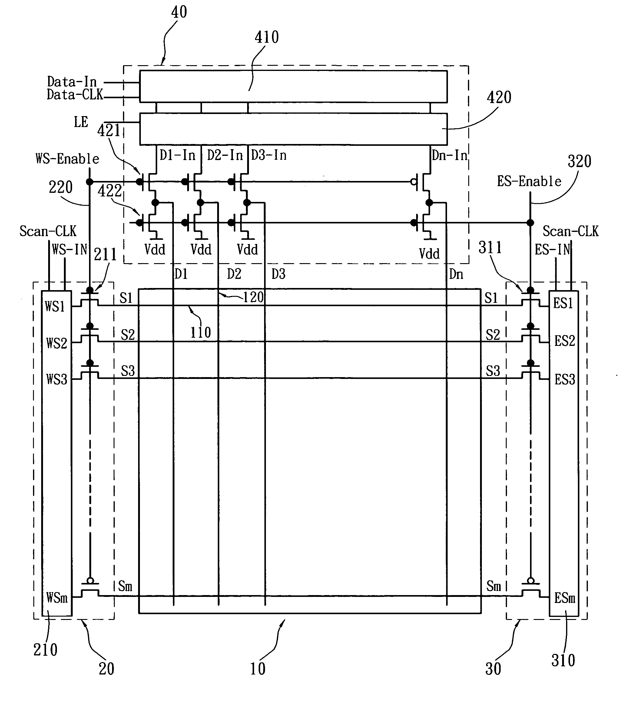
[0020] A description of the content and the technology of this invention along with drawings is made in detail as follows:

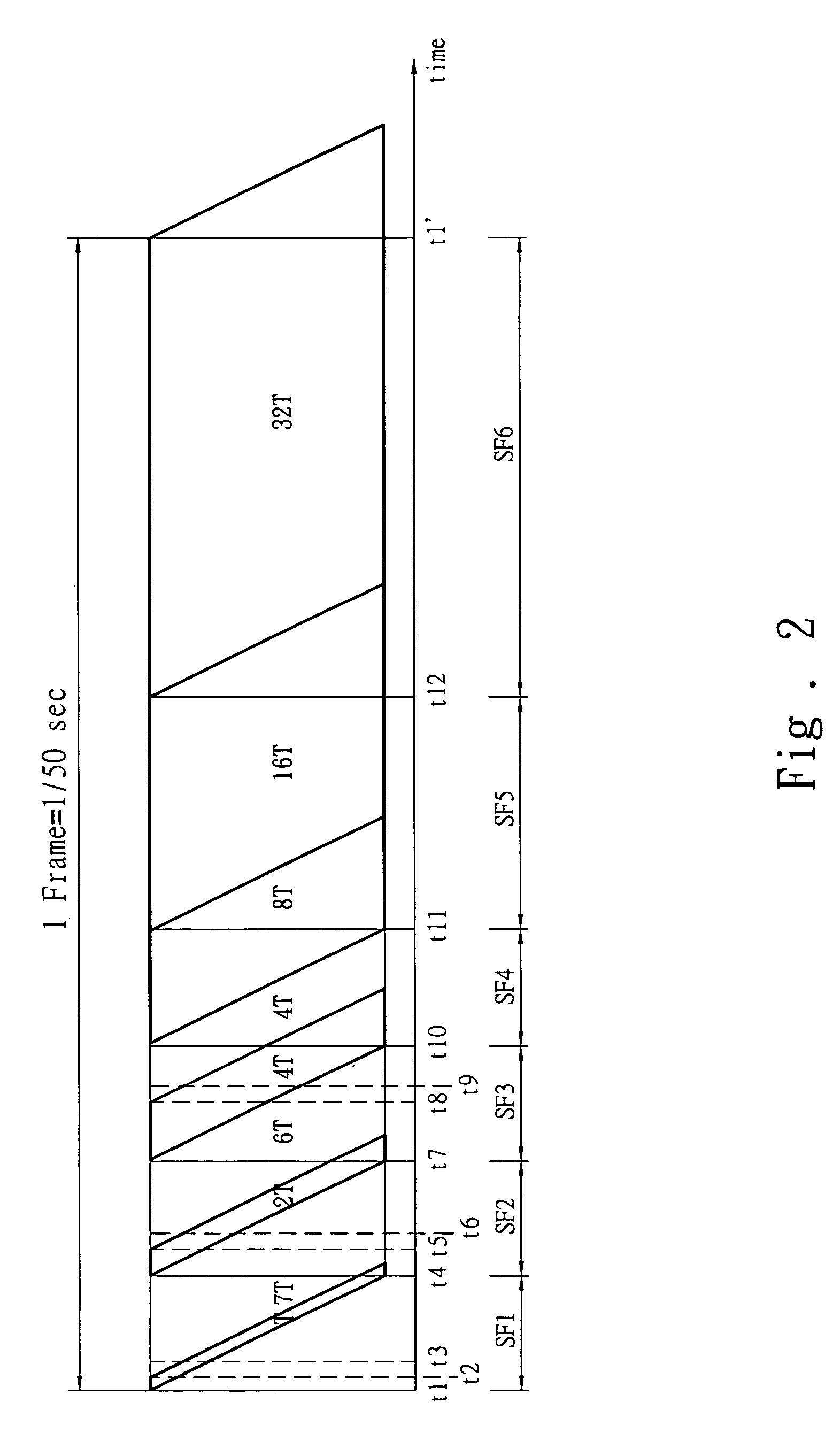
[0021] Refer to FIG. 2 for a high time utility rate driving structure. The feature of this driving method is that pixels on the scan line enter the data display phase immediately after the scan line finishes data writing. And we can find that two actions need to be realized at time point t3. One is to execute the writing of a certain scan line and the other is to execute the erasing of another scan line. If a multiple scan driving circuit and a data driving circuit is designed, the driving method of FIG. 2 would be put into practice successfully.

[0022] Due to the limitation of scan frequency, some scan lines have finished the data display phase in a certain sub-frame, however, some scan lines are still waiting for data writing of the sub-frame. Thus, the scan lines that have completed the data display have to start to execute the data erasing. Take FIG. 2 as an...


PUM


Abstract

A driving apparatus of a multiple-scanning driving circuit relating to a simple pixel structure of 2T1C (2 TFTs and 1 capacitor) includes a write-scan circuit, an erase-scan circuit and a data driving circuit. A write-enable line connected to the write-scan and the data driving circuits is used to control the signals of these two circuits. One erase-enable line connected to the erase-scan and the data driving circuits is used to control the signals of these two circuits. Thus, a circuit system of time-multiplex multiple write-scan and erase-scan is completed to solve the problems of a low time utility rate and an insufficient luminance in a digital driving AMOLED system.

Description

FIELD OF THE INVENTION [0001] This invention relates to driving method for an active matrix organic light emitting display. More particularly, the invention is directed to improve the problem of a low time utility rate in a digital driving system for an active matrix organic light emitting display (AMOLED). BACKGROUND OF THE INVENTION [0002] Organic Light Emitting Displays (OLED) can be divided into passive matrix and active matrix according to driving methods. The so-called active matrix OLED (AMOLED) is to use a thin film transistor (TFT) and the capacitor to store signals and control the luminance and the gray scale of OLED. [0003] For driving technology at present, development of AMOLED has two directions; one is the analog method and the other is the digital way. The reason why digital driving was developed is because TFT elements with uniform features (e.g. threshold voltage and mobility) can't be produced through the current LTPS process. Nevertheless, the stringent demands f...

Claims


Application Information

Patent Timeline
IPC IPC(8): G09G3/20G09G3/30G09G3/32
CPCG09G3/2022G09G3/3266G09G3/3291G09G2320/02G09G2310/0205G09G2310/0251G09G2300/0842
Inventor LO, SHIN-TAI
Owner WINTEK CORP
Why Eureka
Try Eureka