Single chip, noise-resistant, one-dimensional, CMOS sensor for target imaging

Active Publication Date: 2005-06-23
SYMBOL TECH LLC
View PDF9 Cites 18 Cited by
  • Summary
  • Abstract
  • Description
  • Claims
  • Application Information

AI Technical Summary

Benefits of technology

[0006] Accordingly, it is a general object of this invention to reduce power consumption, and to reduce cost a

Problems solved by technology

The use of several support chips results in more total powe

Method used


Image

  • Single chip, noise-resistant, one-dimensional, CMOS sensor for target imaging
  • Single chip, noise-resistant, one-dimensional, CMOS sensor for target imaging
  • Single chip, noise-resistant, one-dimensional, CMOS sensor for target imaging

Examples


Embodiment Construction

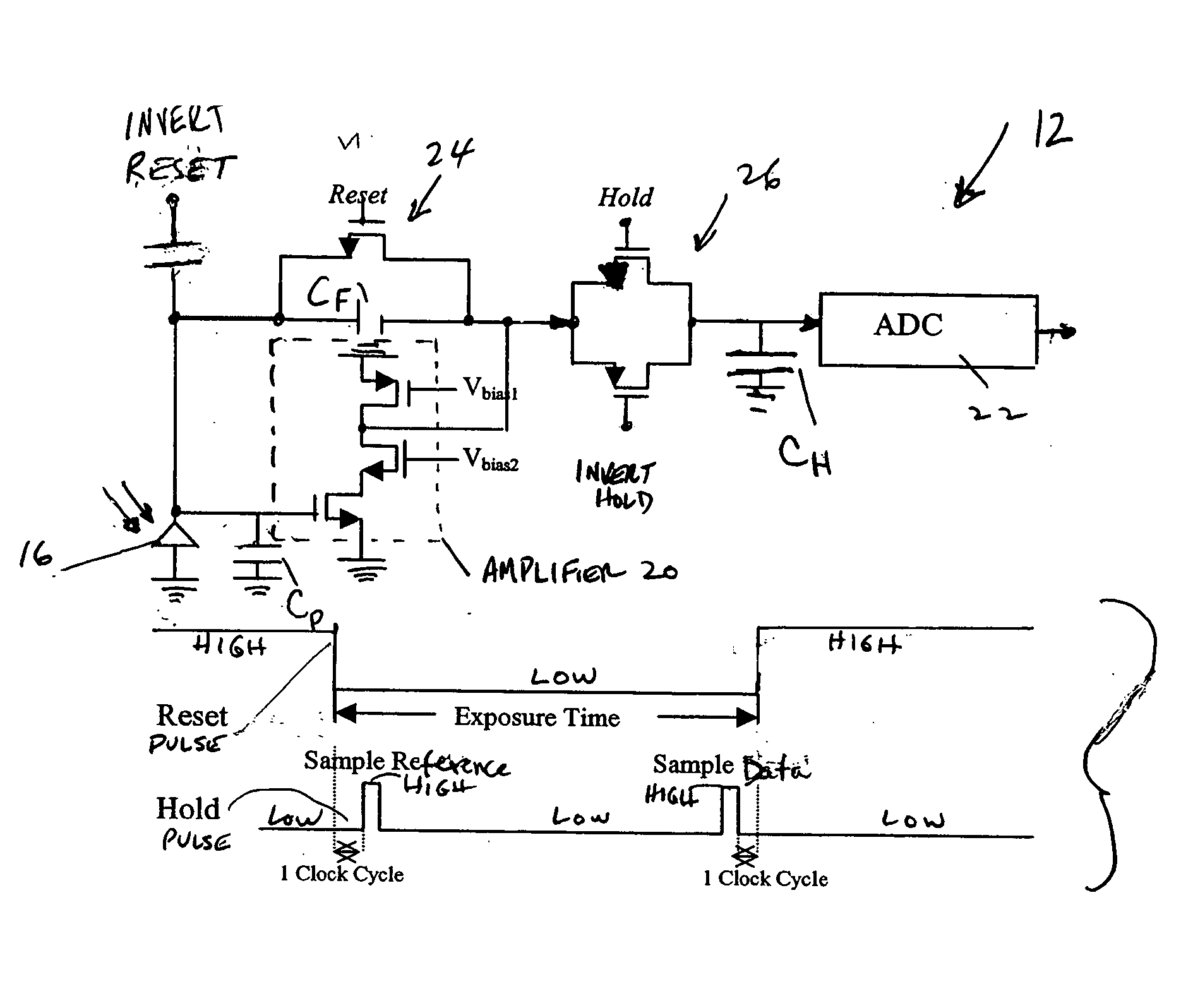
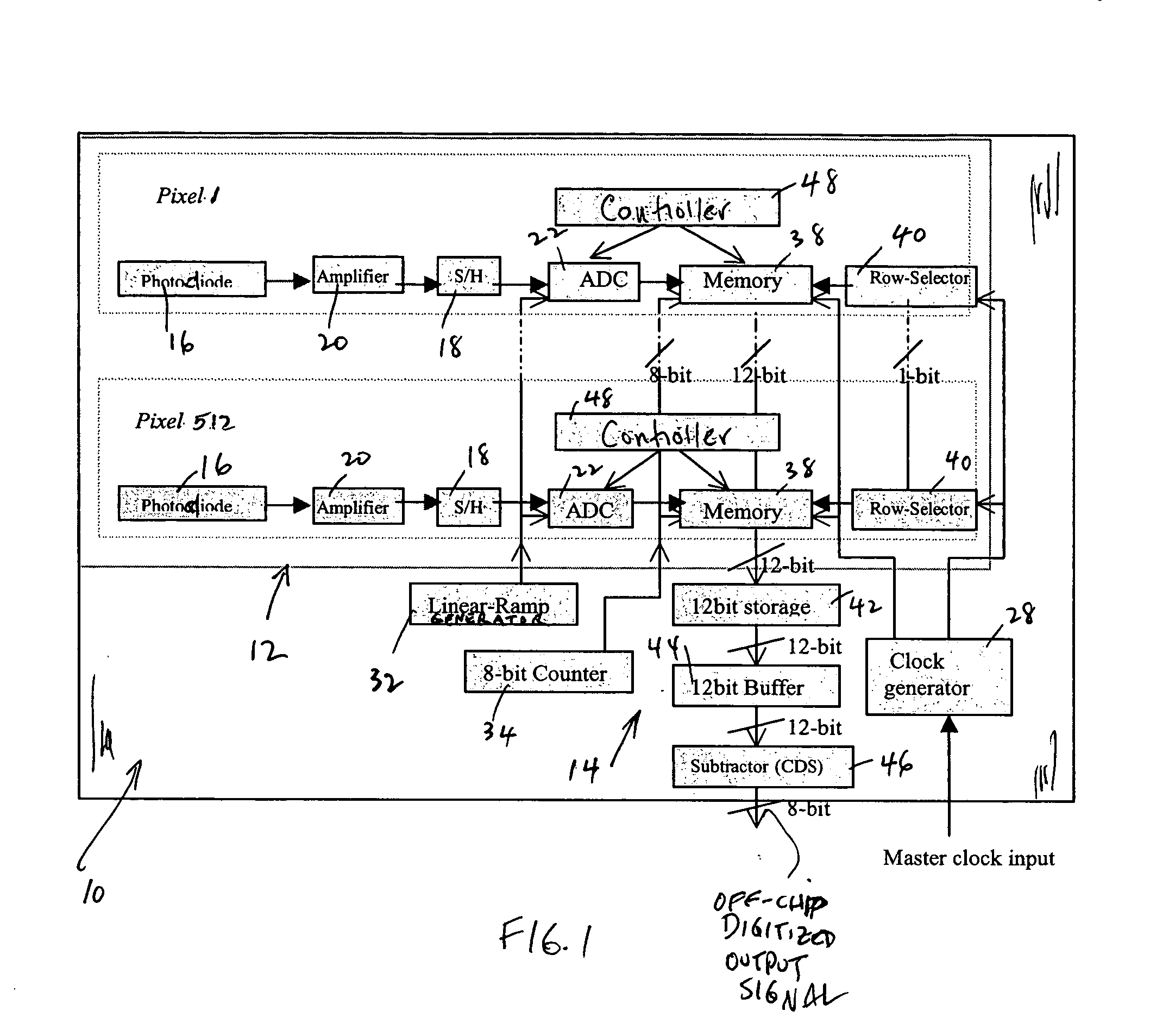
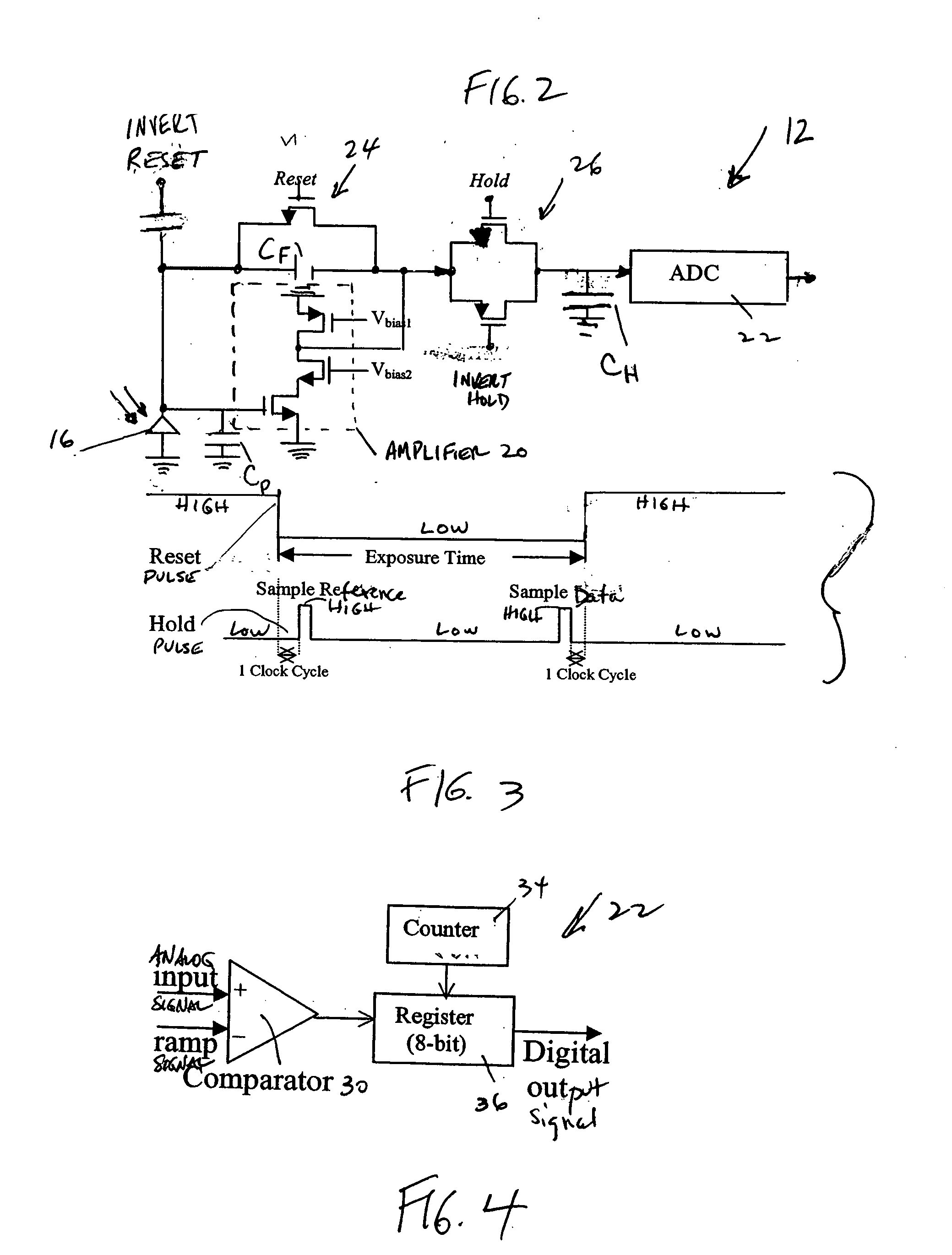
[0022] Referring to FIG. 1, reference numeral 10 generally identifies a single, solid-state, complementary metal-oxide semiconductor (CMOS) chip having an analog front end 12 and a digital back end 14, both the front and back ends being integrated on the same, single CMOS chip 10. The chip is used for imaging a target, especially a one-dimensional coded symbol such as a Universal Product Code (UPC) symbol.

[0023] The front end 12 includes a linear array of pixels, preferably 512 to 4096 pixels in all. Each pixel includes a photodiode 16, a sample-and-hold (S / H) circuit 18, a high gain amplifier20, and an analog-to-digital converter (ADC) 22 which are shown in detail in FIG. 2. All the other components in FIG. 1 are part of the digital back end.

[0024] The photodiode 16 converts incident light into an electrical analog signal. The photodiode has a lower white noise, dark current and fixed-pattern noise as compared to a phototransistor. The photodiode generally has a width between 4 μ...


PUM


Abstract

A linear sensor array for imaging coded indicia includes an analog front end and a digital back end integrated on a single CMOS chip. A real-time, correlated double sampling circuit is used for noise suppression.

Description

BACKGROUND OF THE INVENTION [0001] 1. Field of the Invention [0002] The present invention generally relates to electro-optical readers for reading indicia such as bar code symbols and, more particularly, to a noise-resistant, imaging sensor fabricated on a single semiconductor chip as a linear array and operative for imaging one-dimensional symbols. [0003] 2. Description of the Related Art [0004] Both charge-coupled device (CCD) and complementary metal-oxide semiconductor (CMOS) image sensors are used in digital cameras for imaging a target. Each such two-dimensional, solid-state sensor has a multitude or array of cells or pixels for converting incident light into electrons. In a CCD sensor, an accumulated charge of each cell is transported across, and read out of, the array. In a CMOS sensor, one transistor or several transistors at each pixel amplify and move the charge using traditional wires. CCD sensors have excellent light sensitivity and produce high quality images, whereas C...

Claims


Application Information

Patent Timeline
IPC IPC(8): G06K7/01G06K7/10H04N3/00H04N5/353H04N5/361H04N5/363H04N5/365H04N5/374H04N5/378
CPCG06K7/10722H04N5/335H04N5/378H04N5/3745H04N5/3656H04N25/00H04N25/674H04N25/77H04N25/75
Inventor CARLSON, BRADLEYYAN, MEI
Owner SYMBOL TECH LLC
Why Eureka
Try Eureka