Dynamic schottky barrier MOSFET device and method of manufacture

a barrier mosfet and dynamic technology, applied in the field of transistors, can solve the problems of reducing the effective switching speed of the device and reducing the performance of the transistor

Inactive Publication Date: 2005-06-30
SPINNAKER SEMICON
View PDF3 Cites 161 Cited by
  • Summary
  • Abstract
  • Description
  • Claims
  • Application Information

AI Technical Summary

Problems solved by technology

The sub-linear Id-Vd turn-on characteristic of the SB-MOS device increases as the channel length decreases and ca...

Method used


Image

  • Dynamic schottky barrier MOSFET device and method of manufacture
  • Dynamic schottky barrier MOSFET device and method of manufacture
  • Dynamic schottky barrier MOSFET device and method of manufacture

Examples


Embodiment Construction

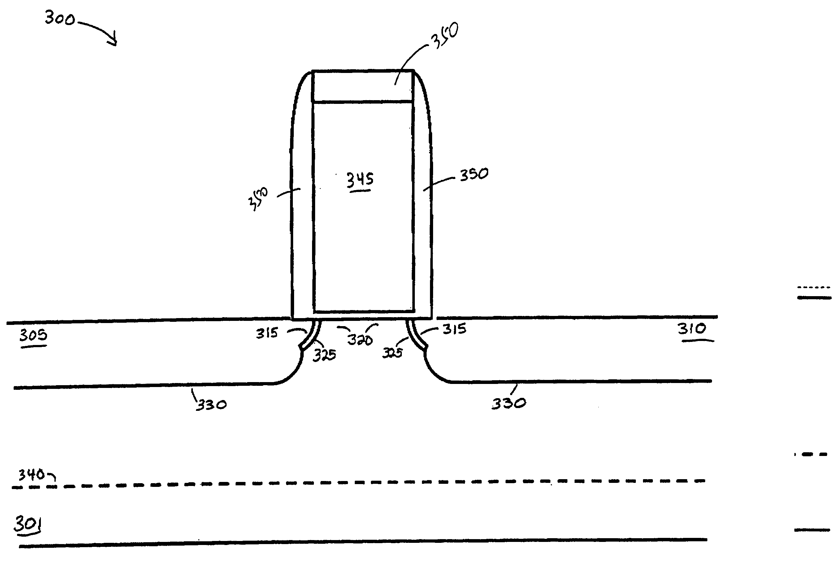
[0029] In general, the present invention provides method of fabrication of SB-MOS devices. In one embodiment of the present invention, the method includes providing a semiconductor substrate and doping the semiconductor substrate and channel region. The method further includes providing a first electrically insulating layer in contact with the semiconductor substrate. The method further includes providing a gate electrode on the first insulating layer, providing a second insulating layer around the gate electrode including the gate electrode sidewalls, and exposing the substrate on one or more areas proximal to the gate electrode. In the present invention, the term proximal is defined as being located within a lateral distance away of approximately 500 Å from one or more said objects. For example, in the previous sentence, the substrate is exposed in one or more areas proximal to the gate electrode, or the one or more areas are located within a lateral distance away of approximately...


PUM


Abstract

A device for regulating a flow of electric current and its manufacturing method are provided. The device includes metal-insulator-semiconductor source-drain contacts forming Schottky barrier or Schottky-like junctions to the semiconductor substrate. The device includes an interfacial layer between the semiconductor substrate and a metal source and/or drain electrode, thereby dynamically adjusting a Schottky barrier height by applying different bias conditions. The dynamic Schottky barrier modulation provides increased electric current for low drain bias conditions, reducing the sub-linear turn-on characteristic of Schottky barrier MOSFET devices and improving device performance.

Description

CROSS-REFERENCE TO RELATED APPLICATION(S) [0001] This application claims the benefit of and priority to U.S. provisional patent application No. 60 / 513,410, filed Oct. 22, 2003. This application also claims the benefit of and priority to U.S. provisional patent application No. 60 / 514,041, filed Oct. 24, 2003. Each of the above provisional patent applications is incorporated by reference herein in their entirety.FIELD OF THE INVENTION [0002] The present invention relates to devices for regulating the flow of electric current, and has specific application to the fabrication of these devices in the context of an integrated circuit (“IC”). More particularly, it relates to a transistor for regulating the flow of electric current having metal source and / or drains forming Schottky-barrier or Schottky-like contacts to a channel region. BACKGROUND OF THE INVENTION [0003] One type of transistor known in the art is a Schottky-barrier metal oxide semiconductor field effect transistor (Schottky-b...

Claims


Application Information

Patent Timeline
IPC IPC(8): H01L21/336H01L29/06H01L29/08H01L29/78
CPCH01L29/0653H01L29/0895H01L29/7839H01L29/66636H01L29/66643H01L29/6656
Inventor SNYDER, JOHN P.LARSON, JOHN M.
Owner SPINNAKER SEMICON
Why Eureka
Try Eureka