Image display device

Active Publication Date: 2005-06-30
SAMSUNG DISPLAY CO LTD +1
View PDF1 Cites 27 Cited by
  • Summary
  • Abstract
  • Description
  • Claims
  • Application Information

AI Technical Summary

Benefits of technology

[0011] The light emitting control switch means makes it can set a non-emission period of light between two consecutive frames by controlling a light-on time of the light emitting means in one frame. By setting an appropriate non-emission period of light, the afterimage effect that had appeared on the human visual property will lessen sufficiently within this non-emission period of light. Accordingly, the images for continuing two frames will not be superposed visually as mentioned above, which permits a smooth animated image display.
[0013] This construction controls a light-on period of the light emitting means at a point of time by the value of the analog signal voltage written in the capacitance means of each pixel so as to achieve a gradation display for animated images or the like. Therefore, it is possible to sufficiently suppress the irregularities of display quality between the pixels, which was the problem for the conventional technique that attains a gradation display by analogously controlling the emission intensity of the light emitting means.

Problems solved by technology

The conventional technique can not provide an especially satisfactory display quality of animated images or sufficiently suppresses the irregularities of display quality between pixels.
The conventional example does not concern a satisfactory display quality of animated images.
However, in such a display method, the human eyes are apt to detect the images for continuing two frames so as to visually superimpose them, owing to the afterimage effect of the visual property, which will present unnatural animated images referred as frame retaining.
This means that the conventional technique also produces brightness unevenness like gain irregularities in each of the pixels, even if the Vth irregularities of the drive TFT 204 can be cancelled (if there are the irregularities of current drive capability due to the irregularities of mobility in the drive TFT 204).
Generally, there are large irregularities between individual devices of the TFTS, and it is very difficult to suppress the irregularities between the individual devices, especially when multiple TFTs are packed in a pixel.
Therefore, the conventional technique can not sufficiently suppress the generation of brightness unevenness due to irregularities of display quality between the pixels.

Method used


Image

  • Image display device
  • Image display device
  • Image display device

Examples


first embodiment

[0039] The first embodiment of the invention is described with reference to FIG. 1 through FIG. 3.

[0040] First, the total construction of this embodiment is discussed with reference to FIG. 1.

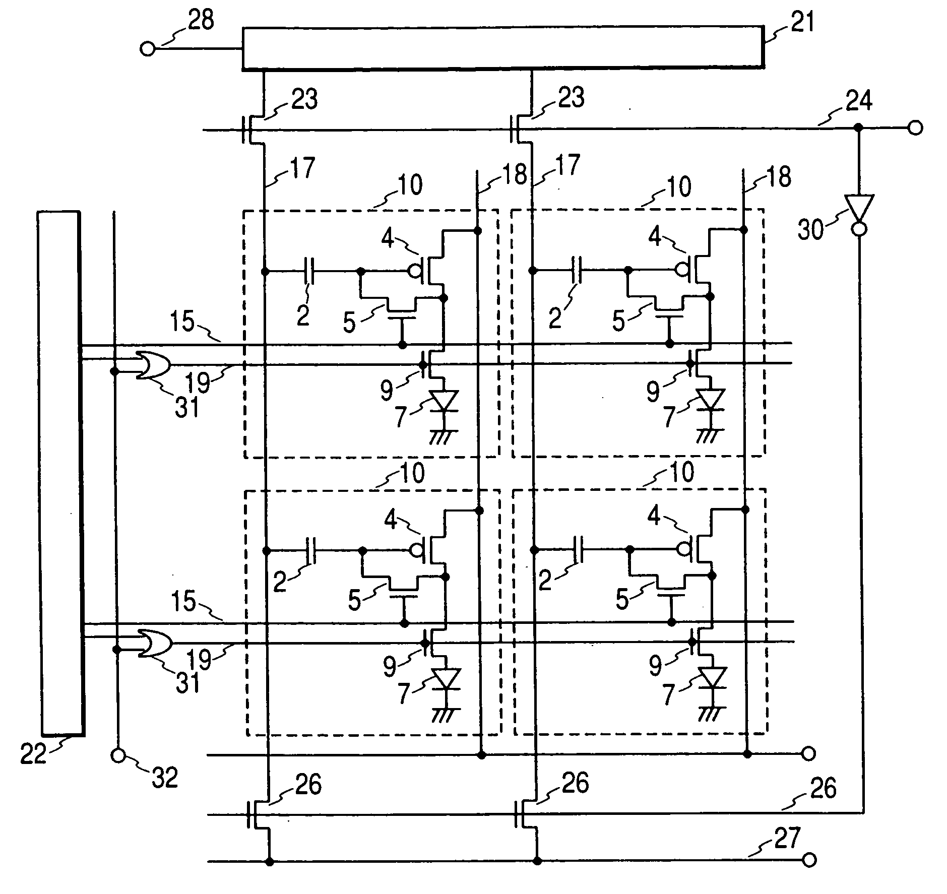
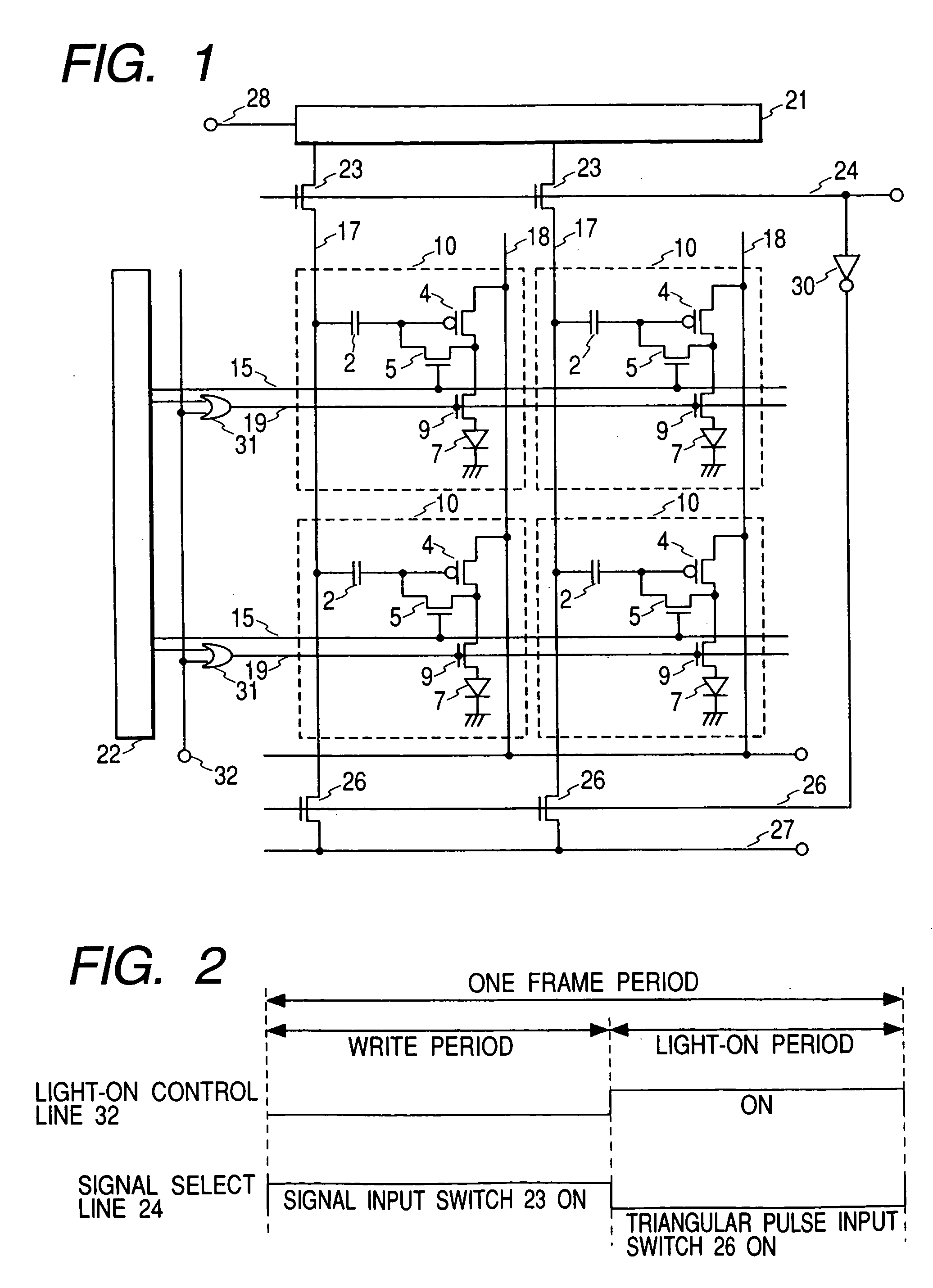
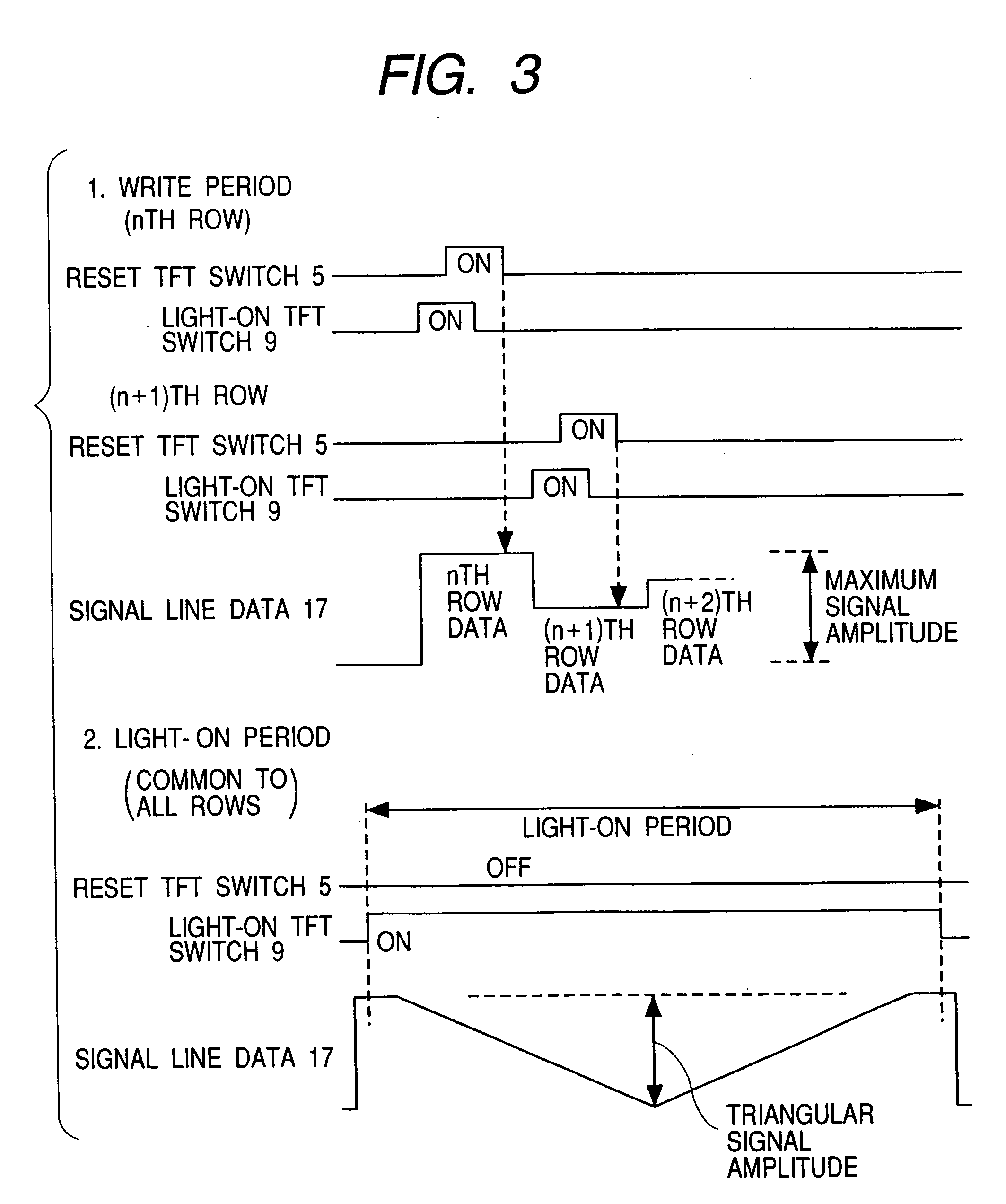
[0041]FIG. 1 illustrates a configuration of an OLED (Organic Light Emitting Diode) display panel of the first embodiment. Pixels 10, each having an OLED 7 as a pixel luminous object, are arrayed in a matrix form on a display unit. Each pixel is connected to the drive circuits furnished surrounding the display unit through a reset line 15, signal line 17, and a light-on switch line 19, etc. The reset line 15 is connected to the scanning output of a gate drive circuit 22, the signal line 17 is connected to a signal drive circuit 21 through a signal input switch 23, and to a triangular pulse input line 27 through a triangular pulse input switch 26. To the signal drive circuit 21 is connected a signal input line 28 that inputs an analog signal voltage. Since the signal drive circuit 21 is an anal...

second embodiment

[0056] The second embodiment of the invention is described with reference to FIG. 4 and FIGS. 5(a) and 5(b).

[0057]FIG. 4 illustrates the configuration of a pixel 40 in the second embodiment.

[0058] The whole construction and the operation of this embodiment are basically the same as those of the first embodiment, except for a reset TFT switch 41 and a light-on TFT switch 42 being composed of p-channel MOS transistors. Accordingly, the description of the whole construction and the operation is omitted, and the reset TFT switch 41 and light-on TFT switch 42, the distinctive features of this embodiment, is explained hereunder.

[0059]FIG. 5(a) illustrates the cross-sectional structure of the reset TFT switch 41, and FIG. 5(b) illustrates the cross-sectional structure of the OLED drive TFT 4 and the light-on TFT switch 42. As described in the first embodiment, both the TFTs are formed by means of the low temperature polycrystalline silicon TFT process. First, on a glass substrate 50 an ...

third embodiment

[0062] The third embodiment of the invention is described with reference to FIG. 6.

[0063]FIG. 6 illustrates the configuration of a pixel 59 in the third embodiment.

[0064] The whole construction and the operation of this embodiment are basically the same as those of the first embodiment, except for an OLED drive TFT 60 being composed of an n-channel MOS transistor, and the cathode and anode of an OLED 61 being connected in reverse. Accordingly, the description of the common construction and the operation is omitted. The OLED drive TFT 60, the OLED 61, and the distinctive features of this embodiment are explained hereunder.

[0065] To an electrode 62 opposite to the OLED 61 is applied with a higher voltage than that of the power supply line 18, and the source of the OLED drive TFT 60 is connected to the power supply line 18 (the same circuit connection as that of the first embodiment). However, since the OLED drive TFT 60 is the n-channel MOS transistor, the upper / lower relation of t...


PUM


Abstract

The invention provides an image display device that has an especially satisfactory display quality for animated images, and sufficiently suppresses the irregularities of display quality among pixels. The image display device includes a light emitting drive means that drives a light emitting means, based on an analog display signal inputted to the pixels, and a light emitting control switch for controlling a light-on or light-off of the light emitting means on one end of the light emitting drive means in each pixel.

Description

FIELD OF THE INVENTION [0001] The present invention relates to an image display device that provides a high quality image display. The invention specifically relates to an image display device that possesses an especially satisfactory display quality of animated images of the like and sufficiently suppresses the irregularities of display quality between pixels. BACKGROUND OF THE INVENTION [0002] A conventional technique will be described with reference to FIG. 23 and FIG. 24. [0003]FIG. 23 illustrates a pixel configuration of a poly-silicon TFT light emitting display device that uses the conventional technique. Pixels each having an organic light emitting diode (OLED) 207 as a pixel luminous object are arrayed on a display unit in a matrix form. However, FIG. 23 illustrates only one pixel in order for simplification. The pixel 210 is connected to an external drive circuit through a selection line 211, a data line 217, a power supply line 218, and so forth. In the pixel 210, the data...

Claims


Application Information

Patent Timeline
IPC IPC(8): H01L51/50G09F9/30G09G3/20G09G3/30G09G3/32H01L27/32
CPCG09G3/2014G09G5/10G09G3/3258G09G3/3283G09G3/3291G09G2300/0417G09G2300/0809G09G2300/0819G09G2300/0842G09G2300/0852G09G2300/0861G09G2310/027G09G2310/065G09G2310/066G09G2320/0257G09G2320/0261G09G2320/043G09G3/3208G09G3/3233G09G3/30G09G3/32G09G5/18G09G2300/0408G09G2300/0426G09G2300/0439G09G2300/0876G09G2310/062G09G2320/0233G09G2320/0242G09G2320/0626
Inventor AKIMOTO, HAJIMEMIKAMI, YOSHIROUKINUGAWA, KIYOSHIGENISHITANI, SHIGEYUKISHIBA, TAKEO
Owner SAMSUNG DISPLAY CO LTD
Why Eureka
Try Eureka