Circuit arrangement design method and circuit arrangement design program

a circuit arrangement and design method technology, applied in the direction of cad circuit design, program control, instruments, etc., can solve the problems of extreme increase of the number of design processes, signal transmission delay, and the influence of wiring arrangement design on the whole circuit layout regarding connections between circuit cells, so as to improve wiring efficiency and improve wiring efficiency. , the effect of improving wiring efficiency

Inactive Publication Date: 2005-06-30
FUJITSU LTD
View PDF7 Cites 4 Cited by
  • Summary
  • Abstract
  • Description
  • Claims
  • Application Information

AI Technical Summary

Benefits of technology

[0013] performing a logic conversion of logic, the logic forming a circuit arrangement where a cell arrangement and a connection arrangement between cells are provisionally arranged prior to a detailed mounting design, and thereby wiring efficiency is improved.
[0014] According to the present invention, in a LSI circuit design, for example, logic and mounting information is read in, virtual wiring is performed according to the information, a wiring efficiency improvable part is extracted from the result, virtual wiring correction is performed by performing wiring conversion and logic conversion, and conversion of the total wiring amount and the signal propagation delay amount accompanying the correction is simulated, so that a logic design and mounting design in which the wiring efficiency is improved can be obtained.
[0015] That is to say, according to the present invention, in the LSI circuit design, for example, prior to a detailed mounting design, arrangement of necessary cells and c...

Problems solved by technology

There is a tendency that the influence on whole circuit layout by wiring arrangement design regarding connections between circuit cells cannot be ignored due to recent high integration of circuits.
In addition, there is another problem, namely sign...

Method used


Image

  • Circuit arrangement design method and circuit arrangement design program
  • Circuit arrangement design method and circuit arrangement design program
  • Circuit arrangement design method and circuit arrangement design program

Examples


Embodiment Construction

[0027] A description is next given, with reference to FIG. 1 through FIG. 10B, of embodiments of the present invention.

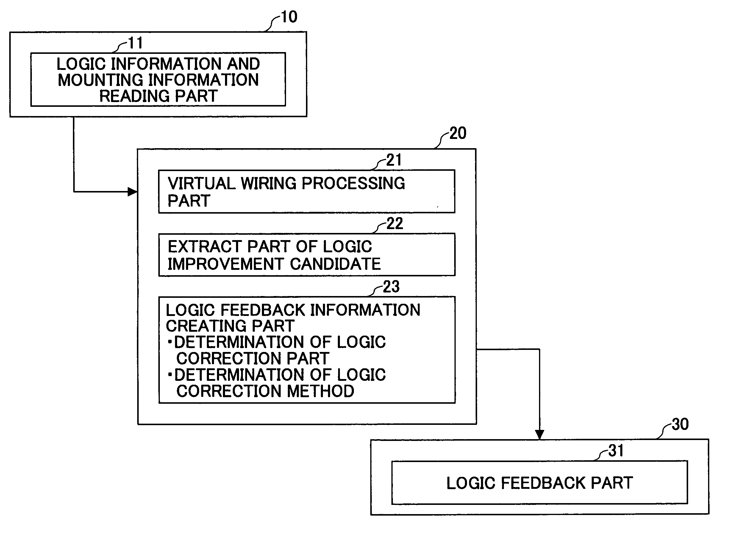
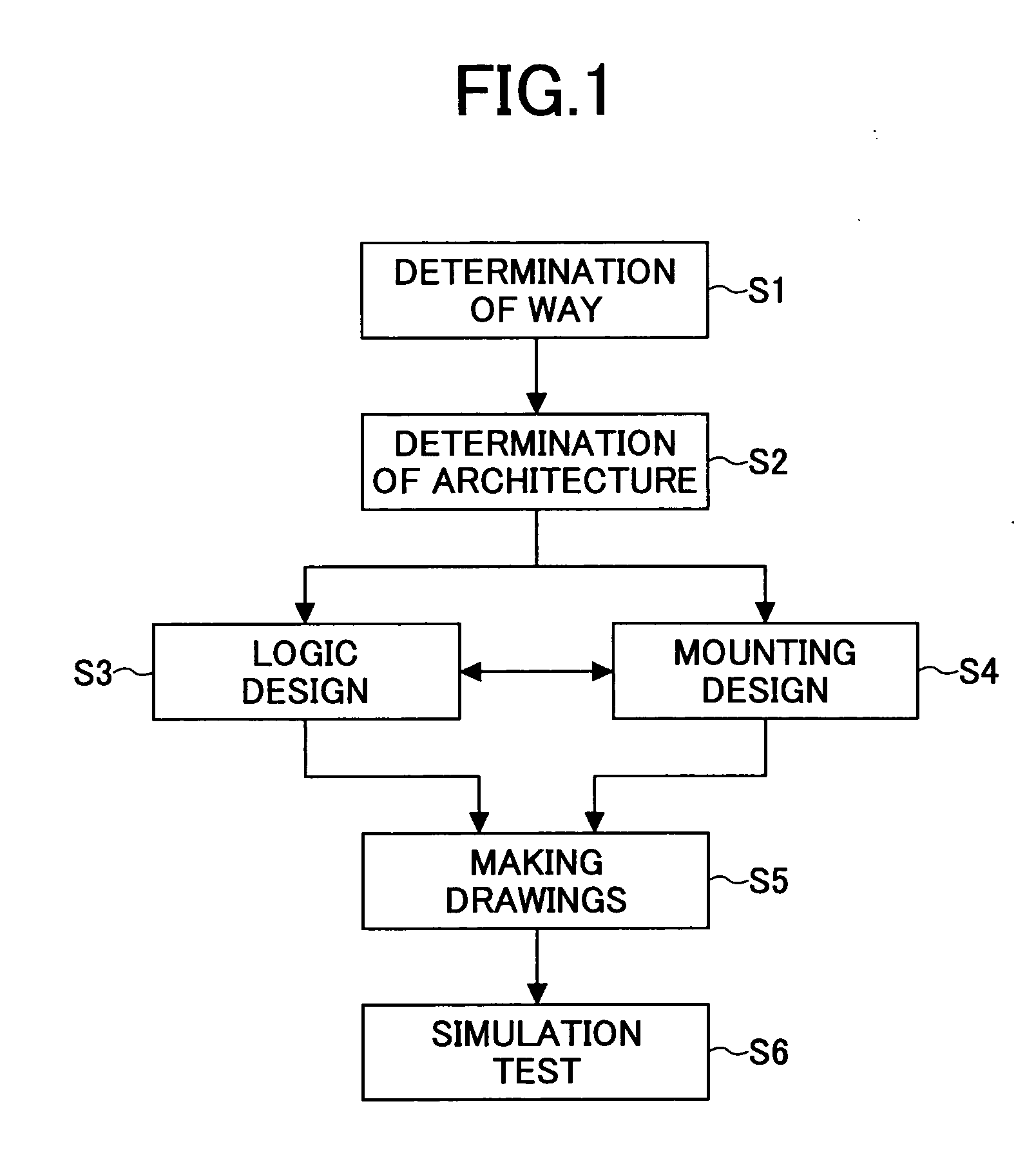
[0028]FIG. 1 is a flowchart showing an example of LSI circuit design processes where the present invention is applied. In step S1, a basic way of a LSI circuit is determined following a request from a user. In step S2, a proper architecture satisfying the way determined in step S1 is examined. In step S3, a logic design is implemented based on the architecture obtained in step S2. In step S4, a mounting design is implemented based on the logic. It is preferable that the logic design and mounting design be performed by closely relating them to each other and that design information be fed-back to each other so that a proper mounting design can be achieved. After the proper mounting design is obtained, design drawings of the design are made in step S5. Based on the design drawings, a detailed action simulation test is performed in step S6.

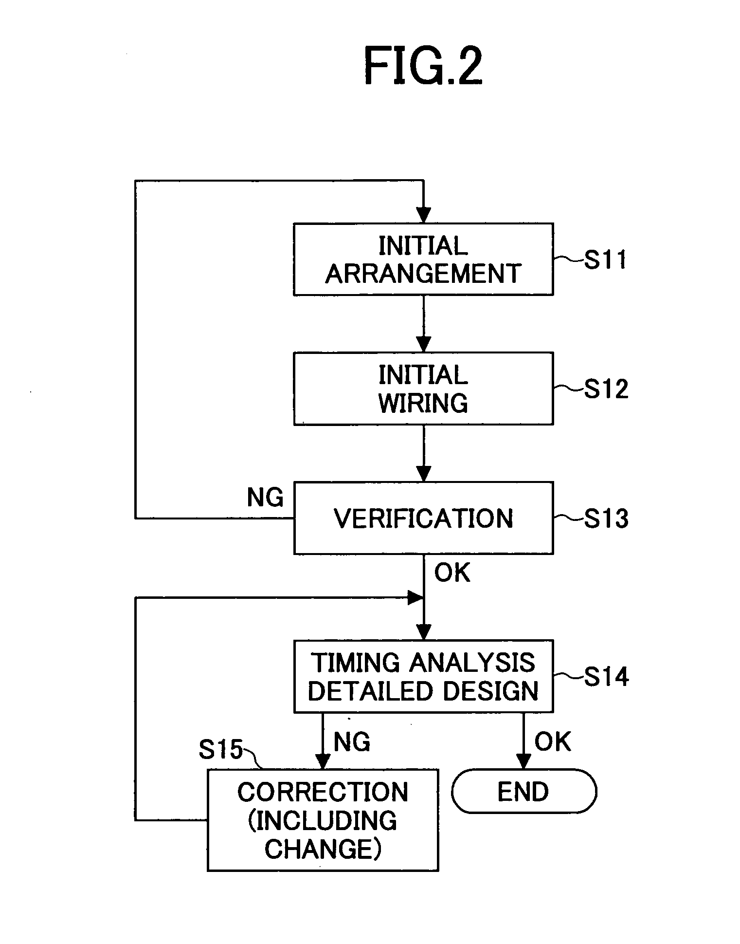
[0029]FIG. 2 is a flowchart...


PUM


Abstract

A circuit arrangement design method includes a step of performing a logic conversion of logic, the logic forming a circuit arrangement where a cell arrangement and a connection arrangement between cells are provisionally arranged prior to a detailed mounting design, and thereby wiring efficiency is improved.

Description

CROSS-REFERENCE TO RELATED APPLICATION [0001] This application is a U.S. continuation application filed under 35 USC 111(a) and claiming benefit under 35 USC 120 and 365(c) of PCT application No. JP2003 / 002515 filed on Mar. 4, 2003. The foregoing application is hereby incorporated by reference. BACKGROUND OF THE INVENTION [0002] 1. Field of the Invention [0003] The present invention generally relates to circuit arrangement design methods and circuit arrangement design programs, and more particularly, to a circuit arrangement design method and circuit arrangement design program, whereby the number of design steps can be effectively decreased in mounting design of a large-scale integrated (LSI) circuit or the like. [0004] 2. Description of the Related Art [0005] There is a tendency that the influence on whole circuit layout by wiring arrangement design regarding connections between circuit cells cannot be ignored due to recent high integration of circuits. Because of this, it becomes ...

Claims


Application Information

Patent Timeline
IPC IPC(8): G06F17/50
CPCG06F17/5068G06F30/39
Inventor AOKI, KATSUSHIITOH, YASUSHI
Owner FUJITSU LTD
Why Eureka
Try Eureka