Heterojunction bipolar transistor and method for manufacturing the same, and power amplifier using the same

a technology of heterojunction bipolar transistor and manufacturing method, which is applied in the direction of amplifiers, semiconductor devices, electrical apparatus, etc., can solve the problems of drastic deterioration in device characteristics, unstable operation of hbt, and reliability of electrical conduction to the device, so as to achieve and reliable electrical conduction and thermal stability

Inactive Publication Date: 2005-07-21
RENESAS ELECTRONICS CORP
View PDF2 Cites 55 Cited by
  • Summary
  • Abstract
  • Description
  • Claims
  • Application Information

AI Technical Summary

Benefits of technology

[0009] In GaAs type HBT, the present invention utilizes the preferred properties (characteristics) of InGaP as an emitter, and to also obtain ballast properties, utilizes the preferred properties of the AlGaAs ballast resistance layer. However by utilizing the GaAs layer as the buffer layer, the present invention can provide an HBT as described above that satisfies both the need for thermal stability and reliable electrical conduction as HBT properties.
[0014] The present invention is capable of providing a heterojunction bipolar transistor (HBT) capable of both reliable electrical conduction and thermal stability. Another aspect of the present invention is capable of providing a heterojunction bipolar transistor (HBT) manufacturing method capable of achieving both reliable electrical conduction and thermal stability. Still another aspect of the present invention is capable of providing a power amplifier capable of achieving both reliable electrical conduction and thermal stability.

Problems solved by technology

However, the HBT has the problem of unstable operation due to heat in a phenomenon called thermal runaway.
The technology disclosed in WO98 / 53502 had the problem of reliability in electrical conduction to the device.
In other words, a drastic deterioration in device characteristics occurred in HBT containing an AlGaAs ballast resistor layer on top of an InGaP emitter layer.
On the other hand, the problem of unstable operation due to thermal runaway as described above occurred when this type of ballast layer was not used.

Method used


Image

  • Heterojunction bipolar transistor and method for manufacturing the same, and power amplifier using the same
  • Heterojunction bipolar transistor and method for manufacturing the same, and power amplifier using the same
  • Heterojunction bipolar transistor and method for manufacturing the same, and power amplifier using the same

Examples


first embodiment

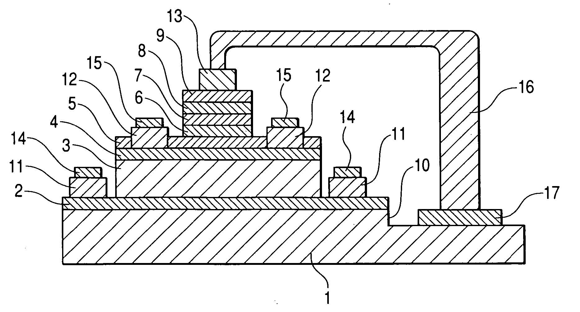
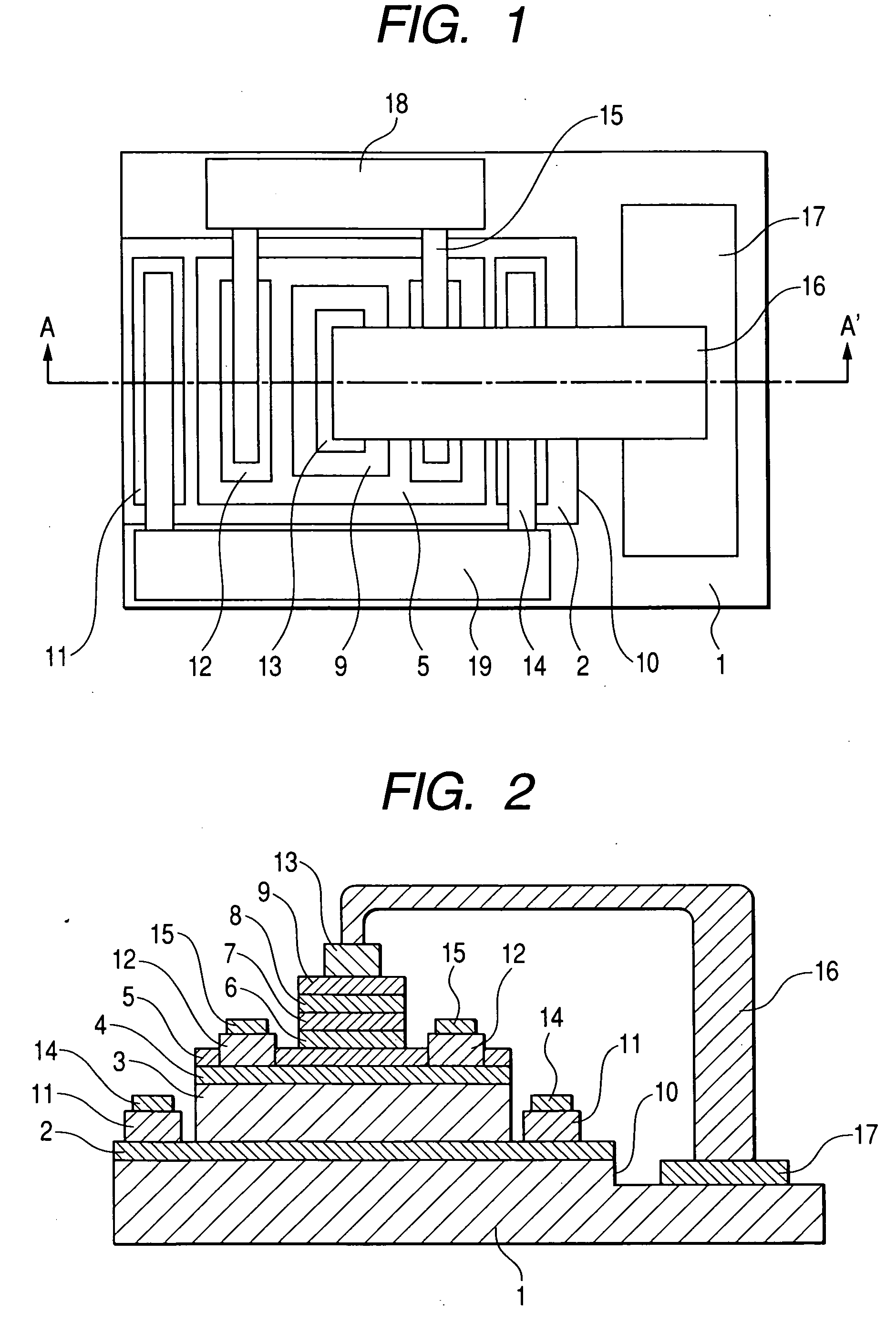
[0047] The HBT according to a first embodiment of the present invention is described next with reference to the accompanying drawings. The present embodiment is for describing the fundamental principle of the present invention and shows a general or concept shape of each section. FIG. 1 is a planar (or flat) view of the HBT of the present invention. A cross sectional view is shown in FIG. 2 taken along the line AA′ in FIG. 1. The emitter size is 108 μm2.

[0048] In the present invention, the generally used items of the related art are sufficient for other essential structural elements than the described emitter layer, GaAs layer, and the ballast resistance layer. For example, a GaAs layer may be used as the base layer and semi-insulating semiconductor substrate, and a GaAs layer as the collector layer.

[0049] An n-type GaAs sub-collector layer (Si concentration 5×1018 cm−3, film thickness 0.6 μm) 2 is formed on the semi-insulating GaAs substrate 1. Layers comprised of an n-type GaAs ...

second embodiment

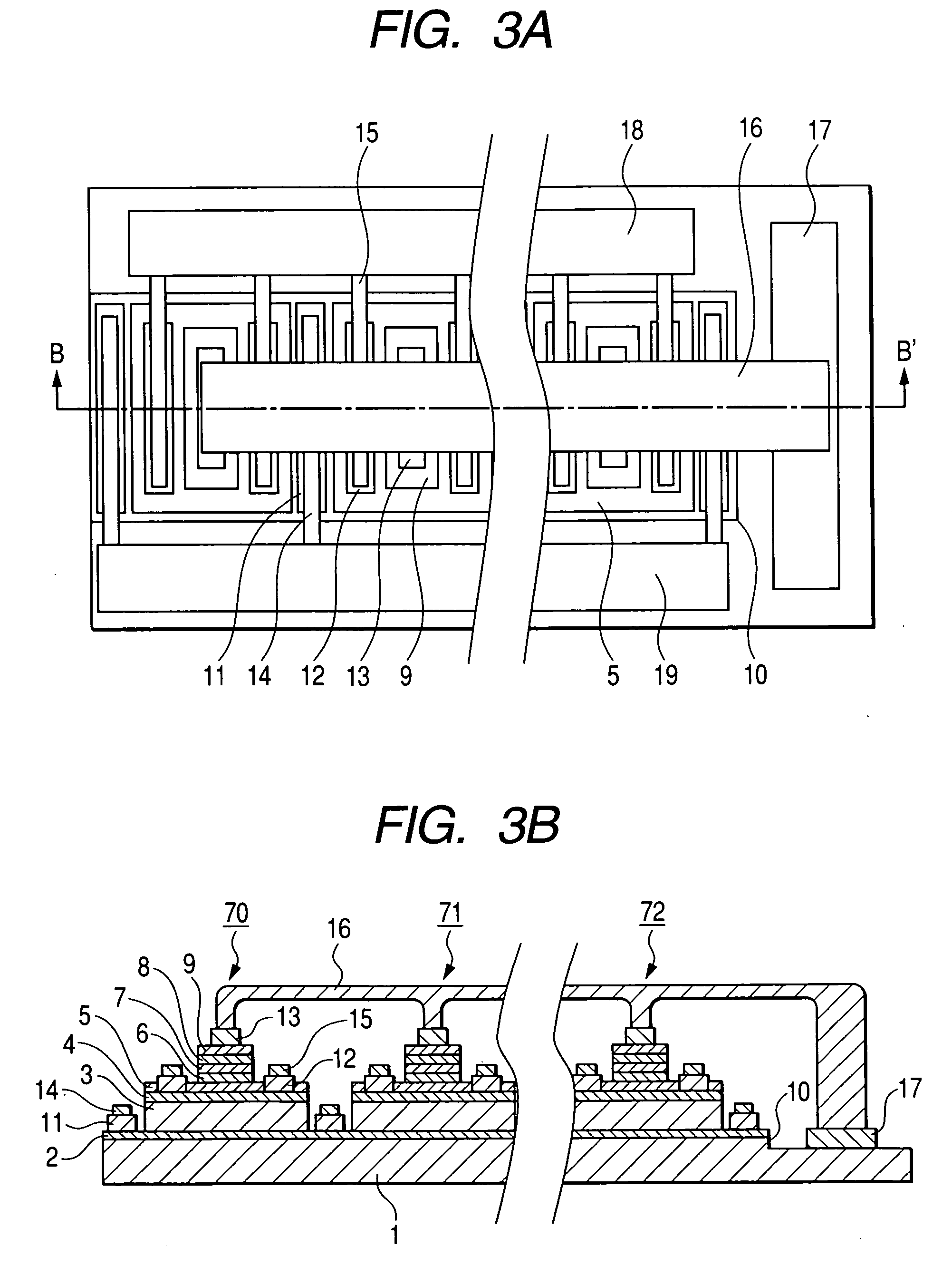
[0056] The second embodiment of the HBT of the present invention is described next while referring to the drawings. The present embodiment is for describing the fundamental principle of the present invention and shows a general or concept shape of each section. The planar structure of the HBT is shown in FIG. 3A. FIG. 3B shows the cross sectional structure taken along the line BB′ in FIG. 3A. The present example is a large power multifinger HBT comprised of basic HBTs wired in parallel. The emitter size of the basic HBT is 108 μM2.

[0057] An n-type GaAs sub-collector layer (Si concentration 5×1018 cm−3, film thickness 0.6 μm) 2 is formed on the semi-insulating GaAs substrate 1. Layers comprised of an n-type GaAs collector layer (Si concentration 1×1016 cm−3, film thickness 1.0 μm) 3, and a p-type GaAs base layer (C concentration 4×1019 cm−3, film thickness 150 nm) 4, and an n-type InGaP emitter layer (InP mol ratio 0.5, Si concentration 3×1017 cm−3, film thickness 30 nm) 5 are forme...

third embodiment

[0062] The typical method for manufacturing the HBT of the present invention is described next while referring to the drawings. The present embodiment is for describing the fundamental principle of the present invention and shows a general or concept shape of each section. Cross sectional views of the device shown from FIG. 4A to FIG. 6C are described while referring to the processes in the method for manufacturing the HBT of the present invention. The present example is a large power multifinger HBT comprised of the basic HBT wired in parallel.

[0063] An n-type GaAs subcollector layer (Si concentration 5×1018 cm−3, film thickness 0.6 μm) 2, an n-type GaAs collector layer (Si concentration 1×1016 cm−3, film thickness 1.0 μm) 3, a p-type GaAs base layer (C concentration 4×1019 cm−3, film thickness 150 nm) 4, an n-type InGaP emitter layer (InP mol ratio 0.5, Si concentration 3×1017 cm−3, film thickness 30 nm) 5, an n-type GaAs layer (Si concentration 3×1017 cm−3, film thickness 90 nm)...


PUM


Abstract

A heterojunction bipolar transistor with InGaP as the emitter layer and capable of both reliable electrical conduction and thermal stability wherein a GaAs layer is inserted between the InGaP emitter layer and AlGaAs ballast resistance layer, to prevent holes reverse-injected from the base layer from diffusing and reaching the AlGaAs ballast resistance layer.

Description

CLAIM OF PRIORITY [0001] The present application claims priority from Japanese application JP 2004-010288 filed on Jan. 19, 2004, and Japanese application JP 2004-287312 filed on Sep. 30, 2004, the contents of which are hereby incorporated by reference into this application. FIELD OF THE INVENTION [0002] The present invention relates to a high reliability heterojunction bipolar transistor, a manufacturing method thereof, and further relates to a power amplifier utilizing that heterojunction bipolar transistor. BACKGROUND OF THE INVENTION [0003] The rapidly growing demand for mobile communications equipment has spurred intensive research and development work on power amplifiers used in communications equipment. Semiconductor transistors utilized in mobile communications equipment power amplifiers include heterojunction bipolar transistors (hereafter abbreviated to HBT), field effect transistors (hereafter abbreviated to FET), and SiMOS (Metal-Oxide-Semiconductors) FET, etc. Among the...

Claims


Application Information

Patent Timeline
Patent Type & Authority Applications(United States)
IPC IPC(8): H01L21/822H01L21/331H01L21/8222H01L27/04H01L27/06H01L27/082H01L29/73H01L29/737H01L29/861H03F3/24
CPCH01L27/0605H01L29/7304H03F2203/21178H03F2200/444H01L29/7371
Inventor OHBU, ISAOKUSANO, CHUSHIROUMEMOTO, YASUNARIKUROKAWA, ATSUSHI
Owner RENESAS ELECTRONICS CORP
Why Eureka
Try Eureka