Silicon carbide imprint stamp

a technology of imprint stamps and silicon carbide, which is applied in the field of manufacturing methods of hardened imprint stamps, can solve the problems of reducing the accuracy of the pattern that is imprinted, the cost of manufacturing the imprint stamp b>200/b> is not recouped, and the micro-casted shape is lost, etc., to achieve the effect of recovering the cost of manufacturing silicon carbide imprint stamps and increasing service li

Inactive Publication Date: 2005-07-28
HEWLETT PACKARD DEV CO LP
View PDF11 Cites 6 Cited by
  • Summary
  • Abstract
  • Description
  • Claims
  • Application Information

AI Technical Summary

Benefits of technology

[0012] Moreover, the silicon carbide imprint stamp has an increased service lifetime; therefore, the cost of manufacturing silicon carbide imprint stamp can be recovered because the imprint stamp can withstand many pressing cycles without wearing out, breaking, or being damaged, unlike the prior imprint stamp that are made from silicon.

Problems solved by technology

One disadvantage to the prior imprint stamp 200 is that the features 203f include the minimum feature size λL.
Another disadvantage of the prior imprint stamp 200 is that the features 203f are susceptible to wearing out and therefore losing their micro-casted shape due to repeated imprinting operations.
Consequently, the imprint pattern will wear out thereby reducing the accuracy of the pattern that is imprinted or the features 203f will be damaged.
Because fabrication of the prior imprint stamp 200 is one of the most crucial and most expensive steps in the entire imprinting lithography process, another disadvantage of the prior imprint stamp 200 is that a cost of manufacturing the imprint stamp 200 is not recouped because the imprint stamp 200 is damaged and / or wears out before an adequate number of pressing steps required to justify the manufacturing cost of the imprint stamp 200 can occur.
Accordingly, the prior imprint stamp 200 is not economical to manufacture.

Method used


Image

  • Silicon carbide imprint stamp
  • Silicon carbide imprint stamp
  • Silicon carbide imprint stamp

Examples


first embodiment

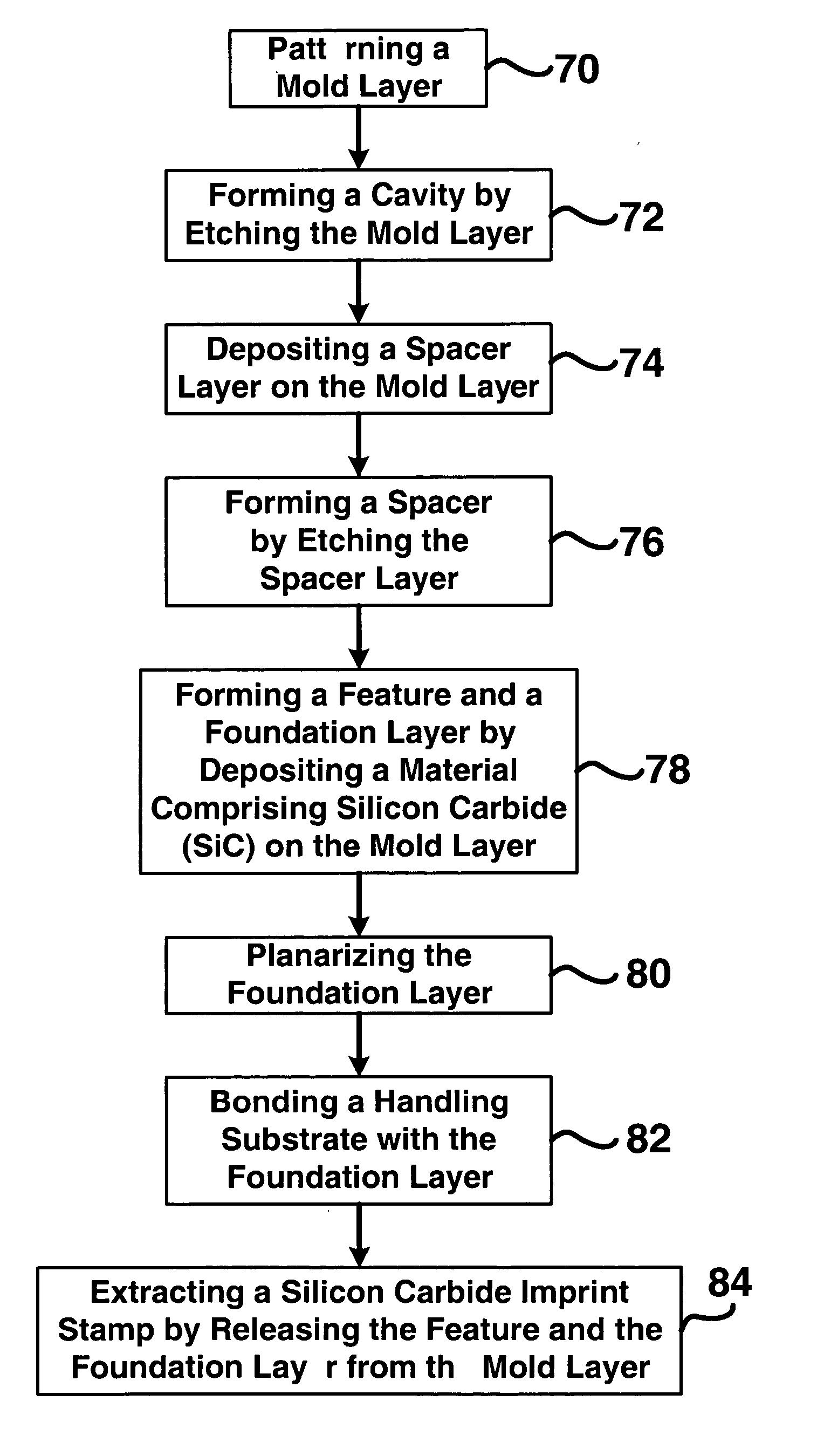
[0051] In FIG. 7, the method of fabricating a silicon carbide imprint stamp includes patterning 70 a mold layer and then forming 72 a cavity in the mold layer by etching the mold layer. A spacer layer is deposited 74 on the mold layer and a spacer is formed 76 by etching the spacer layer. A feature and a foundation layer are formed 78 by depositing a material comprising silicon carbide (SiC) on the mold layer, followed by planarizing 80 the foundation layer. A handling substrate is bonded 82 to the foundation layer. A silicon carbide imprint stamp is formed by releasing 84 the feature and the foundation layer from the mold layer.

second embodiment

[0052] In FIG. 8, in the method of fabricating a silicon carbide imprint stamp, after the planarization 80 as described above in reference to FIG. 7, a glue layer is deposited 90 on the foundation layer. A handling substrate is bonded 92 to the glue layer, followed by releasing 94 the feature and the foundation layer from the mold layer to form silicon carbide imprint stamp.

[0053] In FIGS. 6A and 6B, a silicon carbide imprint stamp 10 includes a handling substrate 15, an optional glue layer 17 connected with the handling substrate 15 and a foundation layer 11 connected with the glue layer 17. If the glue layer 17 is not included, then the foundation layer 11 is connected with the handling substrate 15 (see FIG. 10E). The foundation layer 11 includes one or more features 12 that are connected with the foundation layer 11. The foundation layer 11 and the features 12 are a unitary whole. That is, they (11, 12) are a single piece that is formed as a unit from a micro-casting process tha...


PUM

PropertyMeasurementUnit
feature size λLaaaaaaaaaa
feature depth dmaaaaaaaaaa
feature sizeaaaaaaaaaa

Abstract

A method of fabricating a silicon carbide imprint stamp is disclosed. A mold layer has a cavity formed therein. A spacer is formed in the cavity to reduce a first feature size of the cavity. A casting process is used to form a feature and a foundation layer connected with the feature. The spacer operatively reduces the first feature size of the feature to a second feature size that is less than the lithography limit. The foundation layer and the feature are unitary whole made from a material comprising silicon carbide (SiC), a material that is harder than silicon (Si) alone. Consequently, the silicon carbide imprint stamp has a longer service lifetime because it can endure several imprinting cycles without wearing out or breaking. The longer service lifetime makes the silicon carbide imprint stamp economically feasible to manufacture as the manufacturing cost can be recouped over the service lifetime.

Description

FIELD OF THE INVENTION [0001] The present invention relates generally to a method of fabricating a hardened imprint stamp from a material comprising silicon carbide. More specifically, the present invention relates to a method of forming a hardened imprinting stamp from a material comprising silicon carbide using a casting process and a spacer technique to form imprint patterns that are smaller than a lithography limit. BACKGROUND OF THE ART [0002] Nano-imprinting lithography is a promising technique for obtaining nano-size (as small as a few tens of nanometers) patterns. A key step in forming the nano-size patterns is to first form an imprint stamp (also called an imprinting stamp) that includes a pattern that complements the nano-sized patterns that are to be imprinted by the imprint stamp. [0003] Prior imprint stamps include those made using a micro-casting technique as depicted in FIGS. 1A and 1B, wherein a mold layer 201 is photo lithographically patterned and then etched (e.g....

Claims


Application Information

Patent Timeline
Patent Type & Authority Applications(United States)
IPC IPC(8): C03C25/68
CPCB81C99/009B82Y10/00B82Y40/00G03F7/0002C04B2235/602C04B2235/94C04B35/565
Inventor LEE, HEON
Owner HEWLETT PACKARD DEV CO LP
Why Eureka
Try Eureka