Buffer switch and scheduling method thereof

Inactive Publication Date: 2005-07-28
SAMSUNG ELECTRONICS CO LTD
View PDF14 Cites 12 Cited by
  • Summary
  • Abstract
  • Description
  • Claims
  • Application Information

AI Technical Summary

Benefits of technology

[0041] Furthermore, it is another objective of the present invention to provide a buffer switch and scheduling method thereof in which an increase in load on the operatio

Problems solved by technology

Such an output buffer switch has many advantages in presenting QoS (Quality of Service), but it has limitations that memory speed must be fast and equal to the sum of all input speeds.
Limited memory speed is expected to be a factor in the occurrence of a bottleneck in total speed since the increasing rate of memory speed is lower than that of processor speed due to technical constraints.
The input buffer switch, however, has a limitation in that throughput reaches only 58.6% for uniform input traffic due to HOL (Head-Of-Line) blocking.
The crossbar switch has disadvantages in that the complexity of its implementation increases in proportion to N2 at an N-port crossbar, and control is more complex when guaranteeing QoS because conflicts must be solved at both input ports and output ports.
First, in an input buffer switch, including input buffers that manage queues in

Method used


Image

  • Buffer switch and scheduling method thereof
  • Buffer switch and scheduling method thereof
  • Buffer switch and scheduling method thereof

Examples


Embodiment Construction

[0071] Hereinafter, preferred embodiments of the present invention will be described in detail with reference to the accompanying drawings so that those skilled in the art to which the present invention belongs can easily practice the present invention.

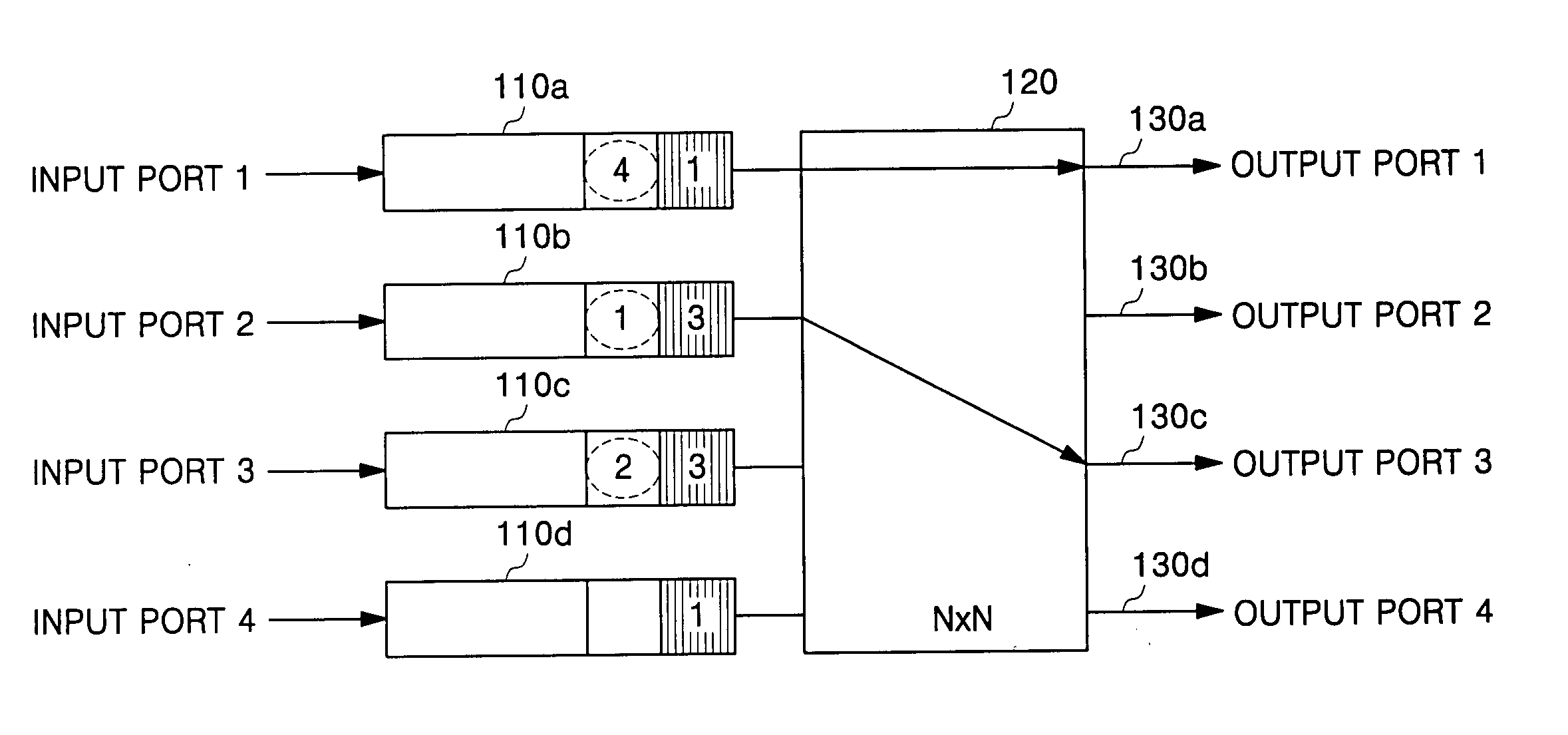
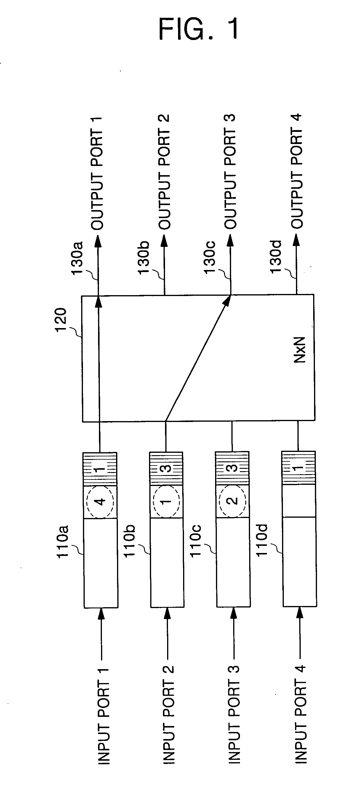
[0072]FIG. 1 illustrates the operation of a typical 4×4 switch, in which data inputted into respective input ports 110a to 110d include a destination port number or destination port numbers.

[0073] In FIG. 1, reference time data inputted into the input port 1110a has a destination port number of 1, reference time data inputted into the input port 2110b has a destination port number of 3, reference time data inputted into the input port 3110c has a destination port number of 3, and reference time data inputted into the input port 4110d has a destination port number of 1.

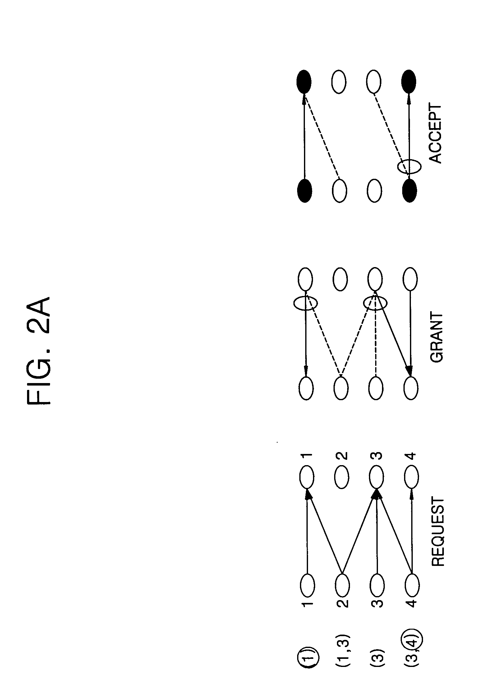
[0074] At this time, a parallel iterative matching (PIM) scheme, which is a typical scheme of a path establishment algorithm is used. Since different input ports 2110...


PUM


Abstract

In a buffer switch and scheduling method thereof, conflict sensing and random selection logic configuration are not required. The buffer switch comprises: input buffer units for converting serial data inputted from respective input ports to parallel data; shift and comparison units for comparing currently stored data to parallel data aligned by the input buffer units, for determining paths to output the data depending on data validity, and for calculating a gating time needed to forward the data; output buffer units for outputting the data received via the input ports at the same speed as the speed at reception; a switching unit for gating paths between the shift and comparison units and the output buffer units; and a control unit for establishing the paths by enabling the input buffer units and the output buffer units for the gating time of relevant buffers depending on the establishment paths and the gating time from the shift and comparison unit.

Description

CLAIM OF PRIORITY [0001] This application makes reference to, incorporates the same herein, and claims all benefits accruing under 35 U.S.C. § 119 from an application for BUFFER SWITCHAND SCHEDULING METHOD THEREOF earlier filed in the Korean Intellectual Property Office on 26 Jan. 2004 and there duly assigned Serial No. 2004-4843. BACKGROUND OF THE INVENTION [0002] 1. Technical Field [0003] The present invention relates to a buffer switch and scheduling method thereof and, more particularly, to a buffer switch and scheduling method thereof in which conflict sensing and random selection logic configuration are not required. [0004] 2. Related Art [0005] A number of studies have been made over past the decade for the purpose of providing a variety of services on an integrated service network. [0006] In particular, many scheduling schemes have been suggested to guarantee a band and a delay to a user who subscribes to a service contract without occurrence of reduced flow which does not c...

Claims


Application Information

Patent Timeline
IPC IPC(8): H04L12/02H04L12/28H04L12/54H04L12/56H04Q11/04
CPCH04L49/101H04L49/3045H04L49/254H04L49/252E03B7/12E04H1/1216
Inventor CHOI, YEONGCHOE, BYUNG-GUKIM, SUN-GI
Owner SAMSUNG ELECTRONICS CO LTD
Why Eureka
Try Eureka