Eureka AIR delivers breakthrough ideas for toughest innovation challenges, trusted by R&D personnel around the world.

Planar optical waveguides with photonic crystal structure

Inactive Publication Date: 2005-08-04
TECHN UNIV OF DENMARK DTU
View PDF1 Cites 4 Cited by
  • Summary
  • Abstract
  • Description
  • Claims
  • Application Information

AI Technical Summary

Benefits of technology

[0009] It is a further disadvantage of prior art PBG-based optical waveguides and devices that a large refractive index difference between the core / cladding features and the background material results in a high sensitivity towards minor structural inaccuracies for certain waveguide or device properties.
[0059] The invention also relates to method of making a planar optical waveguide, in particular a planar optical waveguide, said method comprising steps involving self-writing waveguides. Hereby a particularly advantageous method is provided since the laser beam will create a channel having a changed refractive index, said channel defining an elongated element in e.g. a slab. Hereby, a elongated element positioned in the interior of a slab may be manufactured in a relatively simple and accurate manner.

Problems solved by technology

For compatibility with conventional, silica-based planar optical technology, it is a disadvantage that prior art PBG waveguides and devices incorporates high-index contrasts materials, such as for example voids and silica, or voids and semiconductors.

Method used


Image

  • Planar optical waveguides with photonic crystal structure
  • Planar optical waveguides with photonic crystal structure
  • Planar optical waveguides with photonic crystal structure

Examples


Embodiment Construction

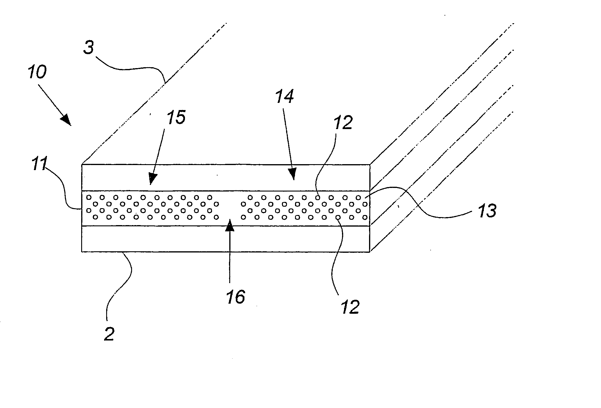
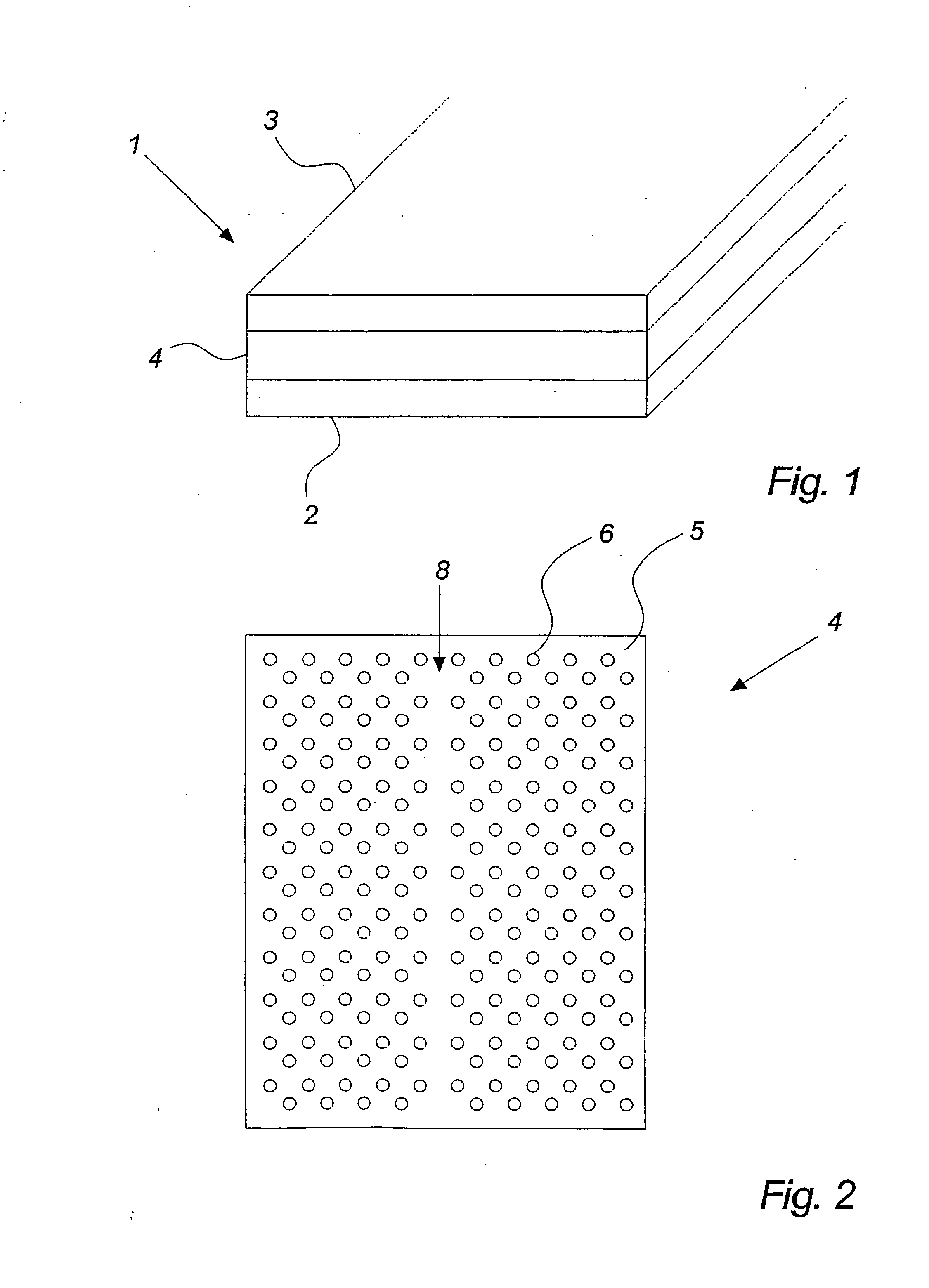
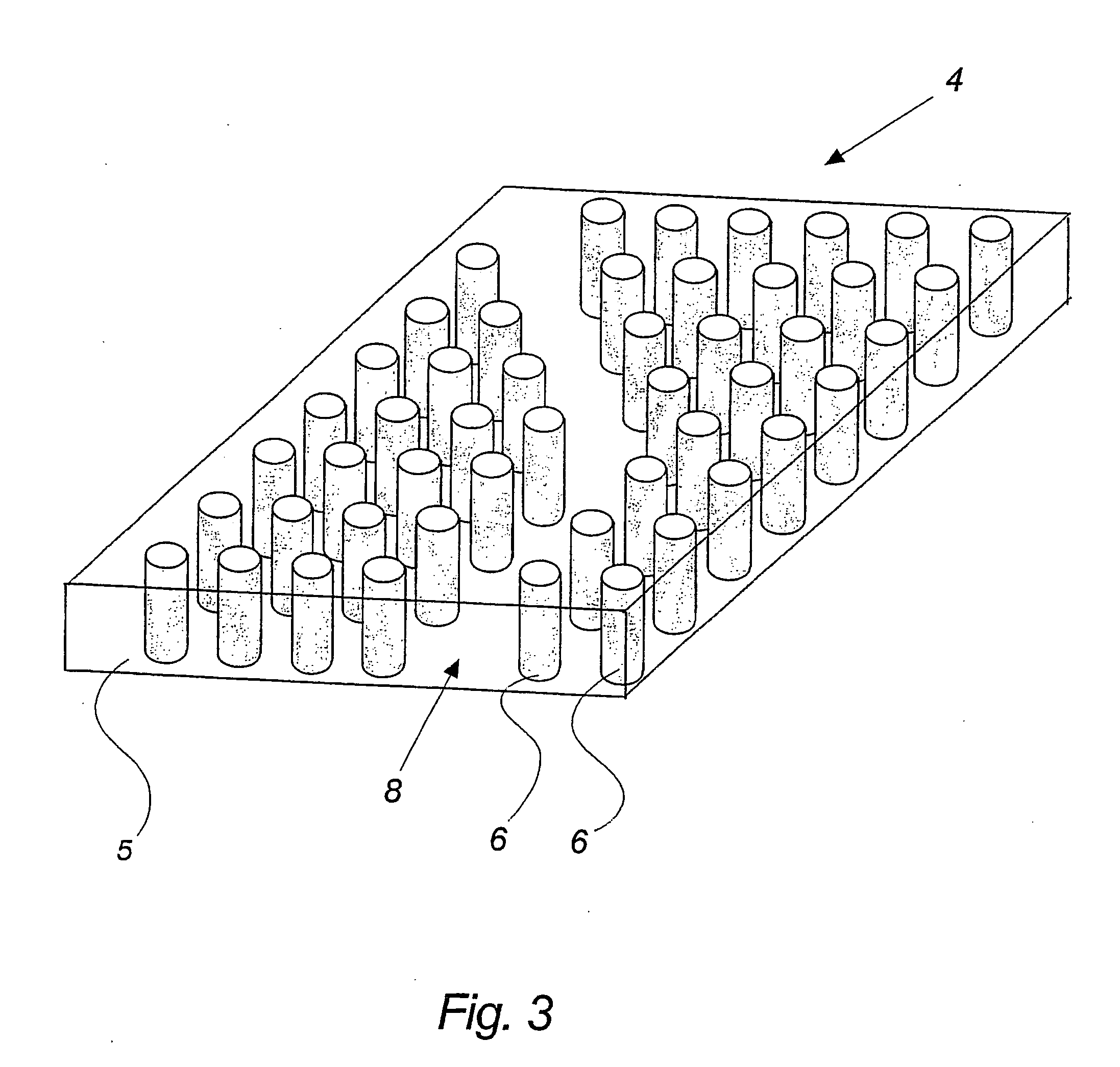
[0079] In the present application it will be distinguished between “refractive index” and “effective refractive index”. The refractive index is the conventional refractive index of a homogeneous material. In this application mainly optical wavelengths in the visible to near-infrared regime (wavelengths from approximately 400 nm to 2 μm) are considered. In this wavelength range most relevant materials for waveguide production (e.g. silica) may be considered mainly wavelength independent, or at least not strongly wavelength dependent. However, for non-homogeneous materials, such as micro-structures, the effective refractive index is very dependent on the morphology of the material. Furthermore the effective refractive index of a micro-structure is strongly wavelength dependent—much stronger than the refractive index of any of the materials composing the micro-structure. The procedure of determining the effective refractive index of a given micro-structure at a given wavelength is well...


PUM


Abstract

Planar optical waveguide comprising a core region and a cladding region comprising a photonic crystal material, said photonic crystal material having a lattice of column elements, wherein at least a number of said column elements are elongated substantially in an axial direction for said core region. The invention also relates to optical devices comprising planar optical waveguides and methods of making waveguides and optical devices.

Description

CROSS-REFERENCE TO RELATED APPLICATION [0001] This application, filed under 35 U.S.C. §363, claims the benefit pursuant to §119(e) of U.S. provisional patent application No. 60 / 364,869 filed on Mar. 15, 2002, the contents of which are herein incorporated by reference in their entirety.FIELD OF THE INVENTION [0002] The present invention relates to planar optical waveguides and devices that operate by photonic bandgap effects. The invention provides a new range of photonic bandgap (PBG) guiding optical waveguides and devices of a new design, which may be implemented in a number of ways and which may be implemented using structures that do need to contain any voids. The optical waveguides and devices covered by the present invention may be employed for a number of applications, including amplifiers and lasers, coupling devices, and sensors. The invention further provides a number of methods for fabricating such waveguides and devices. BACKGROUND OF THE INVENTION [0003] Within the past ...

Claims


Application Information

Patent Timeline
IPC IPC(8): G02B6/10G02B6/122G02B6/124G02B6/13
CPCB82Y20/00G02B6/13G02B6/124G02B6/1225
Inventor BROENG, JESBJARKLEV, ANDERS
Owner TECHN UNIV OF DENMARK DTU
Why Eureka
Eureka Blog
Learn More