Device and method for transferring a pattern to a substrate

a technology of pattern and substrate, applied in the field of patterns transfer devices, can solve problems such as pattern obstruction and plate deformation, and achieve the effect of efficient patterning

Inactive Publication Date: 2005-08-11
OBDUCAT AB SE
View PDF5 Cites 43 Cited by
  • Summary
  • Abstract
  • Description
  • Claims
  • Application Information

AI Technical Summary

Benefits of technology

[0007] The object of the present invention is to provide a...

Problems solved by technology

A large bending of the stamping plates may result in the...

Method used


Image

  • Device and method for transferring a pattern to a substrate
  • Device and method for transferring a pattern to a substrate
  • Device and method for transferring a pattern to a substrate

Examples


Embodiment Construction

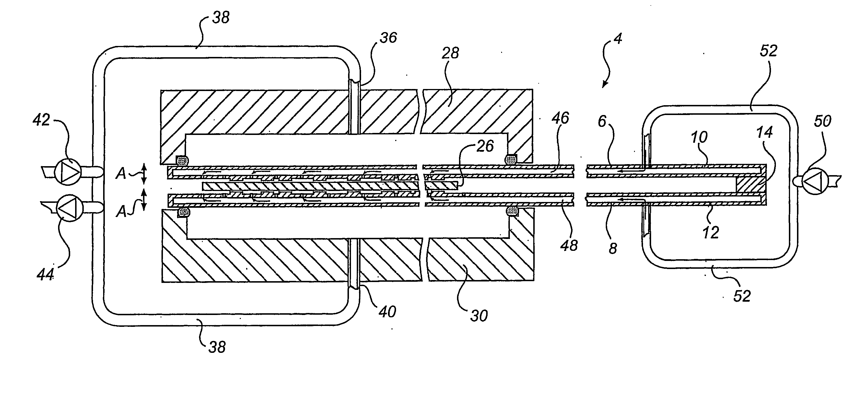
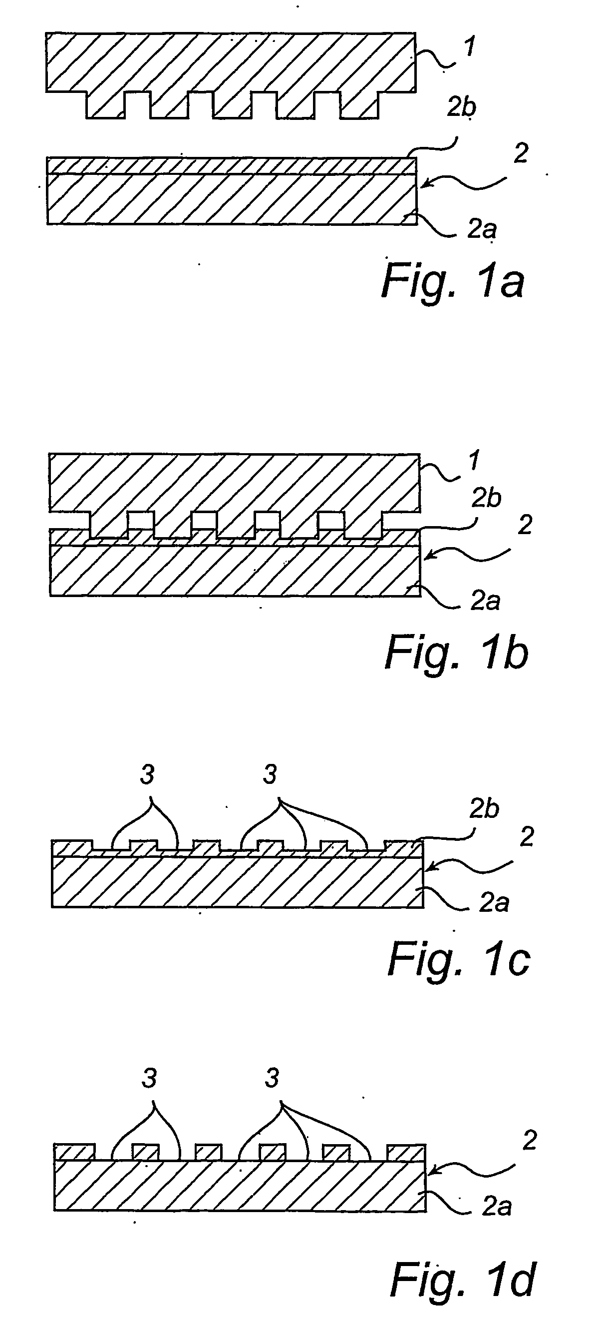
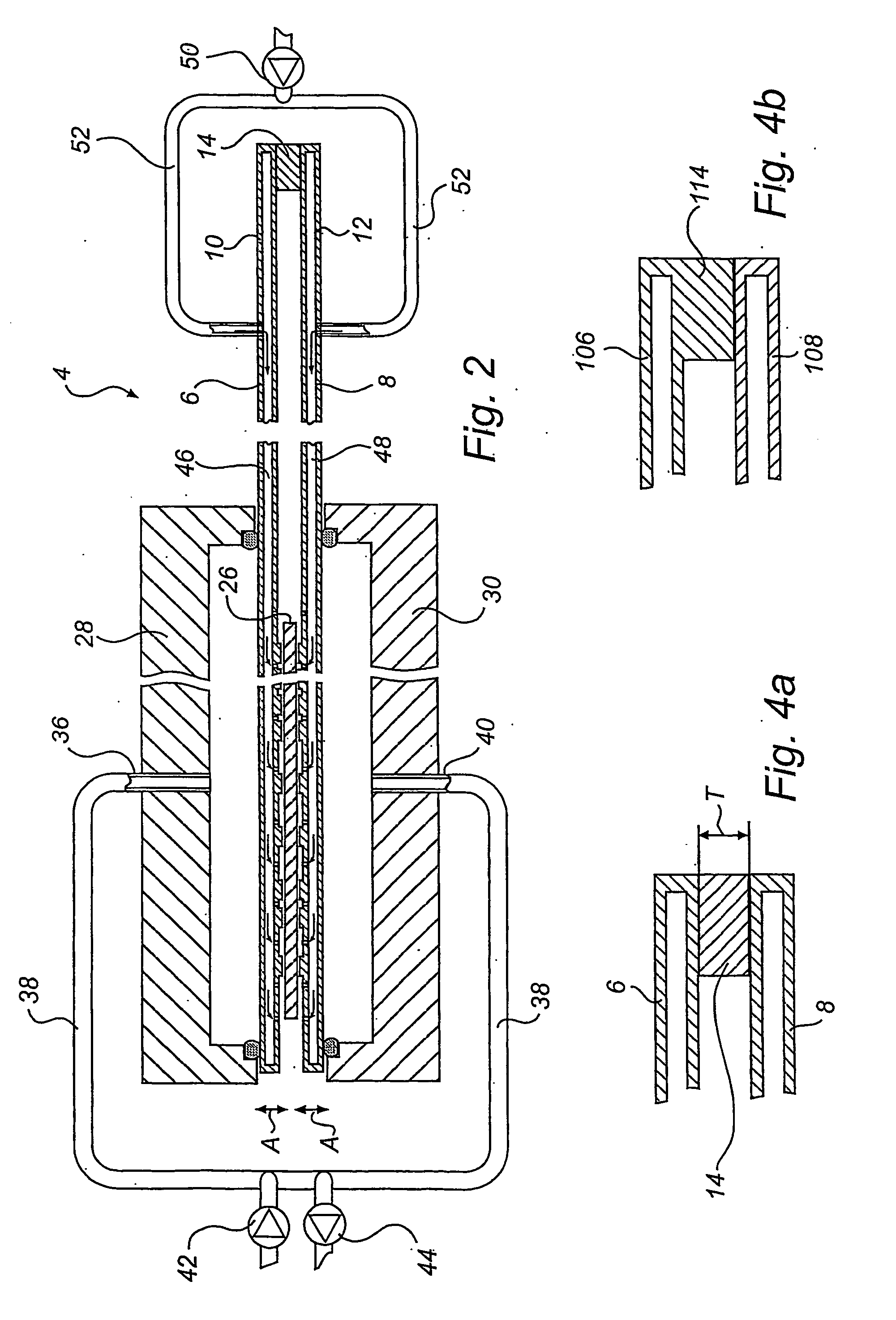
[0029] The present invention relates to nano imprinting, i.e. the forming of patterns in substrates by forcing a stamp having a pattern into contact with a substrate thereby transferring said pattern to the substrate. Examples of products that could be manufactured with the aid of the present invention include hard disks, optical disks, micromechanical devices, microfluid devices and microelectronic devices.

[0030] The term “nano-imprinting” should not be read as referring only to submicron structures, i.e. structures with a size in the range of 0,1-1000 nm. A pattern often includes both submicron structures and structures with a size of up to 100 micron, and larger. The present invention is applicable for forming of patterns comprising submicron structures and / or micron structures. The invention is particularly advantageous when forming patterns comprising submicron structures since these are relatively more sensitive to incorrect positioning of the transferred patterns relative to...


PUM

PropertyMeasurementUnit
Thicknessaaaaaaaaaa
Forceaaaaaaaaaa
Pressureaaaaaaaaaa

Abstract

A device (4) for transferring patterns, especially micro- or nanostructures, to at least two faces of a substrate (26) comprises a first stamping plate (6) having a patterned area provided thereon for forming a first pattern on a first face of said substrate (26), a second stamping plate (8) having a patterned area provided thereon for forming a second pattern on a second face of said substrate (26), and a contacting means (28, 30) for contacting the respective patterned areas of the two stamping plates (6, 8) with the respective faces of said substrate (26). The first and the second stamping plates (6, 8) are aligned with each other and are secured to each other at respective holding areas (10, 12) of the stamping plates (6, 8) located at a distance from the patterned areas.

Description

TECHNICAL FIELD OF THE INVENTION [0001] The present invention relates to a device for transferring patterns, especially micro- or nano-structures, to at least two faces of a substrate. [0002] The invention further relates to a method of transferring patterns, especially micro- or nano-structures, to at least two faces of a substrate and to a substrate having patterns on at least two faces thereof. BACKGROUND ART [0003] A technique for the reproduction of nanostructures, i.e. structures in the order of 1000 nm and smaller, is embossing imprint lithography. In this technique a stamp having a pattern is forced into contact with a substrate. The pattern is transferred to the substrate and the stamp is then removed from the substrate. An example of this method is shown in WO 01 / 69317. In such lithography, the main steps of which are schematically shown in FIGS. 1a-1d, a pattern of nanostructures is transferred from a stamp 1 to an object 2. The object 2 consists of a substrate 2a and, ap...

Claims


Application Information

Patent Timeline
IPC IPC(8): B81C1/00G03F7/00
CPCB81C1/0046G03F7/0002B82Y40/00B82Y10/00
Inventor OLSSON, LENNART
Owner OBDUCAT AB SE
Why Eureka
Try Eureka