Heat dissipating substrate for semiconductor and preparation method thereof

semiconductor technology, applied in the direction of semiconductor devices, solid-state devices, basic electric elements, etc., can solve the problems of difficult to apply the conventional preparation method of a metal pcb to a heat dissipating substrate for a high-power semiconductor, and the corresponding device cannot meet the requirements of high-power semiconductors, etc., to achieve excellent heat dissipation performance, improve insulating strength, and efficient preparation of the hea

Pending Publication Date: 2022-07-14
LEE JONG EUN
View PDF2 Cites 0 Cited by
  • Summary
  • Abstract
  • Description
  • Claims
  • Application Information

AI Technical Summary

Benefits of technology

[0029]In accordance with the embodiments of the present disclosure, it is possible to provide a heat dissipating substrate having a thick electrode metal plate having a thickness of 0.2 mm or more, and a preparation method which can efficiently prepare the heat dissipating substrate.
[0030]Furthermore, it is possible to provide a heat dissipating substrate which has a thick electrode metal plate to accomplish excellent heat dissipating performance and to improve insulating strength, and has high peel strength.
[0031]Furthermore, it is possible to provide a preparation method of a heat dissipating substrate, which can effectively pattern a thick electrode metal plate, and efficiently prepare an eco-friendly heat dissipating substrate for semiconductor, which exhibits excellent insulating performance and high peel strength.
[0032]Furthermore, the preparation method may exclude an etching and plating process which cause environmental pollution, and replace the etching and plating process with a mechanical process which uses or discharges no toxic chemicals and heavy chemicals, thereby preparing a heat dissipating substrate for semiconductor through an eco-friendly process.

Problems solved by technology

Therefore, a considerable amount of heat may be generated from the power module, and cause a malfunction and reliability problem of the corresponding device.
However, it is difficult to apply the conventional preparation method of a metal PCB to a heat dissipating substrate for a high-power semiconductor.
That is because, when the thickness of an electrode metal plate is increased to mount a high-power semiconductor, it is difficult to apply an etching or plating method to cope with the mounting process.
Furthermore, the cross-sectional profile of the electrode pattern may be degraded to easily cause dielectric breakdown.
Moreover, the etching or plating process uses toxic chemicals or heavy metals, thereby causing environmental pollution.

Method used


Image

  • Heat dissipating substrate for semiconductor and preparation method thereof
  • Heat dissipating substrate for semiconductor and preparation method thereof
  • Heat dissipating substrate for semiconductor and preparation method thereof

Examples


first embodiment

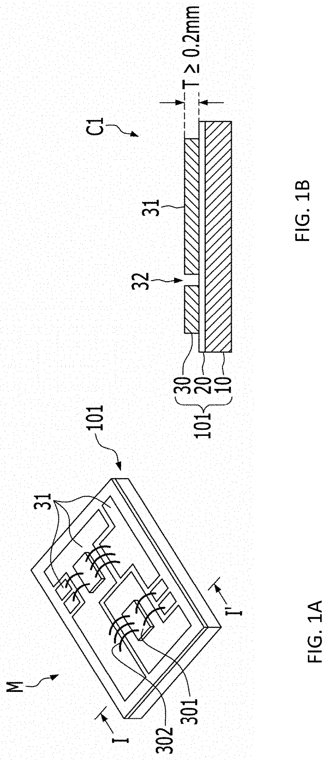
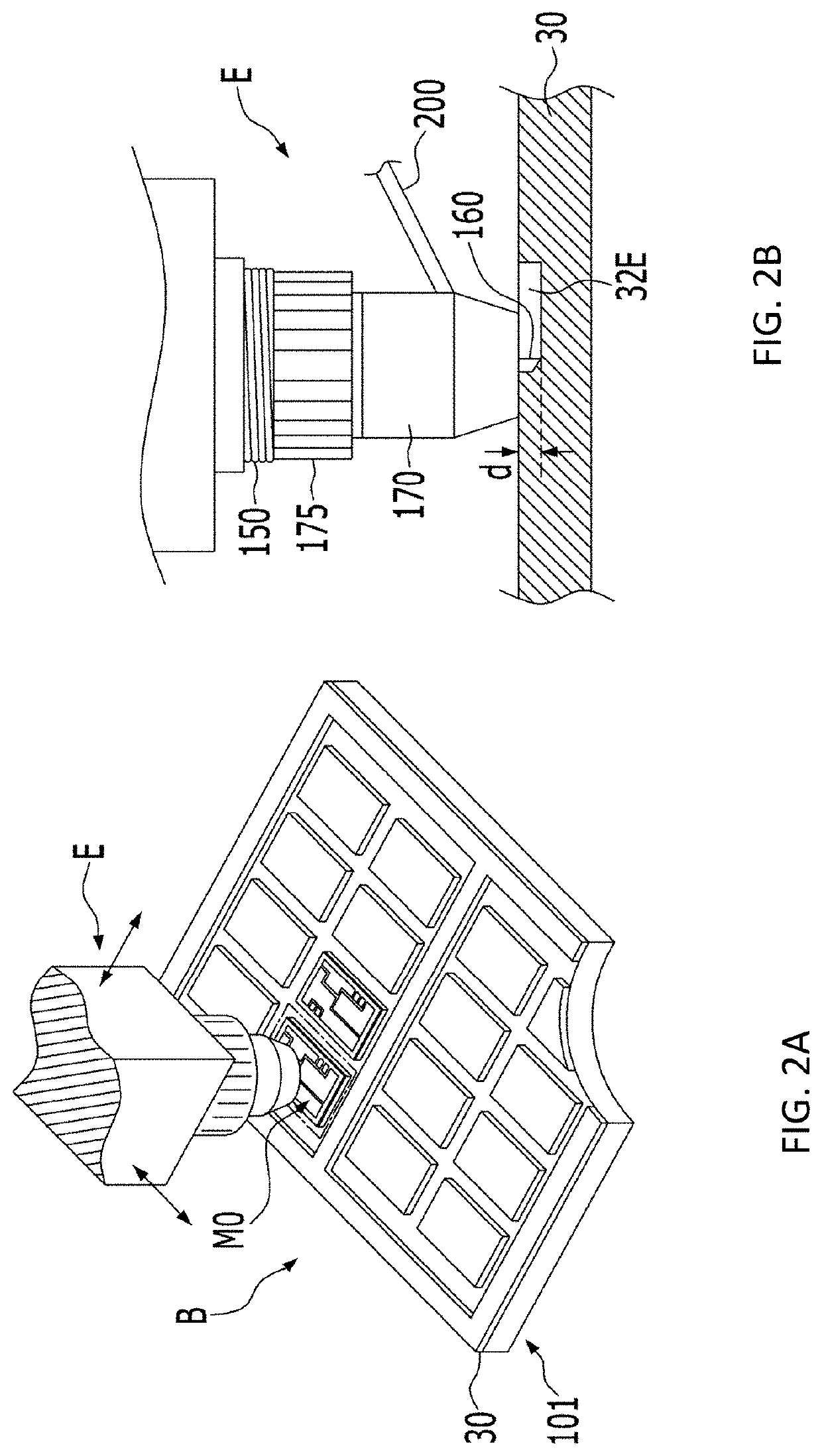
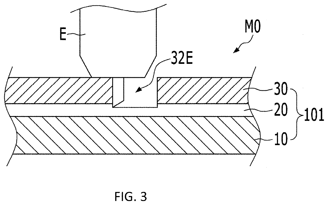
[0060]FIG. 3 illustrates a preparation method of a heat dissipating substrate M0 for semiconductor in accordance with a While a metal base 10, an insulating layer 20 and an electrode metal layer 30 are sequentially stacked from the bottom, a constant depth cutting machine E is used to form a pattern space 32 having a depth that is larger than the thickness of the electrode metal layer 30 and exposes only the insulating layer 20.

second embodiment

[0061]FIGS. 4A to 4C illustrate a preparation method of a heat dissipating substrate for semiconductor in accordance with an embodiment of the present disclosure. FIGS. 4A to 4C illustrate a preparation method of a heat dissipating substrate M1 for semiconductor in accordance with a

[0062]Referring to FIG. 4A, a multilayered heat dissipating substrate 101 in which a metal base 10, an insulating layer 20 and an electrode metal layer 30 are sequentially stacked from the bottom as in the embodiment of FIG. 3 is formed, and an electrode pattern-shaped mask pattern 41 is formed on the top surface of the electrode metal layer 30.

[0063]Referring to FIG. 4B, a constant depth cutting machine E is used to form a groove pattern 32E corresponding to a pattern space in a portion on which the mask pattern 41 is not printed. At this time, a remaining portion having a thickness t of 0.05 mm to 0.1 mm is left at the bottom of the groove pattern 32E

[0064]Referring to FIG. 3C, the remaining portion at ...

third embodiment

[0065]FIGS. 5A to 5C illustrate a preparation method of a heat dissipating substrate for semiconductor in accordance with an embodiment of the present disclosure. FIGS. 5A to 5C illustrate a preparation method of a heat dissipating substrate M1 for semiconductor in accordance with a

[0066]Referring to FIG. 5A, a groove pattern 32E is formed at the top surface of an electrode metal layer 30 through a constant depth cutting machine E. At this time, a remaining portion 320 having a predetermined thickness t is left at the bottom of the groove pattern 32E. The predetermined thickness t is equal to that in the embodiment of FIG. 4. Separately, a substrate having an insulating layer 20 stacked on the top surface of a metal base 10 is prepared.

[0067]Referring to FIG. 4B, the electrode metal layer 30 having the groove pattern 32E formed in FIG. 4A is bonded to the substrate having the insulating layer 20 stacked on the top surface of the metal base 10. During the bonding process, a vacuum ho...


PUM

PropertyMeasurementUnit
thermal conductivityaaaaaaaaaa
thicknessaaaaaaaaaa
thicknessaaaaaaaaaa

Abstract

Provided are a heat dissipating substrate and a preparation method thereof, which can form a precise pattern in a thick electrode metal plate and improve insulating strength and peel strength. heat dissipating substrate for semiconductor may include: an electrode metal plate having a plurality of electrode patterns which are electrically insulated from each other by a pattern space formed therebetween; a metal base disposed under the electrode metal plate, and configured to diffuse heat conducted from the electrode metal plate; an insulating layer formed between the electrode metal plate and the metal base; and an insulating material filled portion configured to fill the pattern space and a peripheral portion outside an electrode pattern group composed of the plurality of electrode patterns, and support the electrode patterns while brought in direct contact with side surfaces of the plurality of electrode patterns.

Description

TECHNICAL FIELD[0001]The present disclosure relates to a heat dissipating substrate for mounting a semiconductor element, a semiconductor module including the same, and a preparation method thereof. More particularly, the present disclosure relates to a heat dissipating substrate which functions as a heat dissipating plate and a circuit board for mounting a semiconductor element, a preparation method of a heat dissipating substrate which has a thick electrode metal plate suitable for mounting a high-power semiconductor element or high-power LED, and structural characteristics of the heat dissipating substrate.BACKGROUND ART[0002]Recently, in the electric power industry, research and development are being actively conducted on the generation, storage, and utilization of new renewable energy such as sunlight generation or wind power generation. Furthermore, research and development are also being actively conducted on the efficiency improvement, stability and energy reduction of vario...

Claims


Application Information

Patent Timeline
Patent Type & Authority Applications(United States)
IPC IPC(8): H01L21/48H01L23/367H01L23/373H01L29/40
CPCH01L21/4871H01L23/367H01L23/3735H01L33/64H01L21/4842H01L21/4828H01L29/401H01L23/49568H01L21/4882H01L23/3672H01L23/3677H01L23/145H01L23/15C04B37/021C04B37/026C04B2237/12C04B2237/365C04B2237/366C04B2237/407H01L2224/49111H01L23/3737H01L23/142H01L23/528
Inventor LEE, JONG EUN
Owner LEE JONG EUN
Why Eureka
Try Eureka