Liquid crystal pixel memory, liquid crystal display, and methods of driving the same

a liquid crystal display and pixel memory technology, applied in the direction of electric digital data processing, instruments, computing, etc., can solve the problems of large power consumption of the driver lsi, inability to achieve uniform distribution of liquid crystal molecules in the liquid crystal layer, and difficulty in enhancing image quality, etc., to achieve high image quality and increase power consumption

Inactive Publication Date: 2005-08-11
ADVANCED LCD TECH DEVMENT CENT
View PDF1 Cites 53 Cited by
  • Summary
  • Abstract
  • Description
  • Claims
  • Application Information

AI Technical Summary

Benefits of technology

[0011] The present invention has been made in order to solve the above-described problems, and the object of the invention is to provide a liquid crystal pixel memory, a liquid crystal display, and methods of driving the same, wherein a high image quality can be obtained without an increase in power consumption.

Problems solved by technology

If the alignment state of liquid crystal molecules is continuously controlled by a unidirectional electric field, non-uniform distribution of liquid crystal molecules occurs in the liquid crystal layer.
Since a parasitic wiring capacitance on the signal lines is charged and discharged with the polarity that is reversed by the driver LSI in cycles of one horizontal scan period, the power consumption of the driver LSI is very large.
Further, in the active matrix liquid crystal display, how to enhance the image quality is also a technical problem to be solved.
If such a number of elements and lines are actually provided within the limited pixel area, the aperture ratio and manufacturing yield will deteriorate.
Thus, it is difficult to provide a low-power-consumption, high-image-quality liquid crystal display at low cost.
In this configuration, an increase in power consumption of the signal line driver LSI cannot be suppressed.

Method used


Image

  • Liquid crystal pixel memory, liquid crystal display, and methods of driving the same
  • Liquid crystal pixel memory, liquid crystal display, and methods of driving the same
  • Liquid crystal pixel memory, liquid crystal display, and methods of driving the same

Examples


first embodiment

[0046] A transmission-type active matrix liquid crystal display according to a first embodiment of the present invention will now be described with reference to the accompanying drawings.

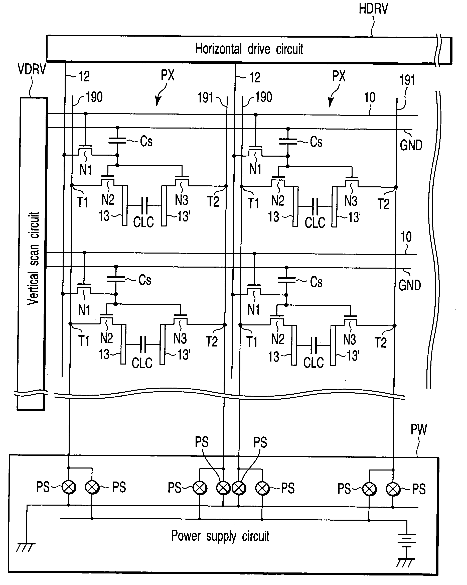
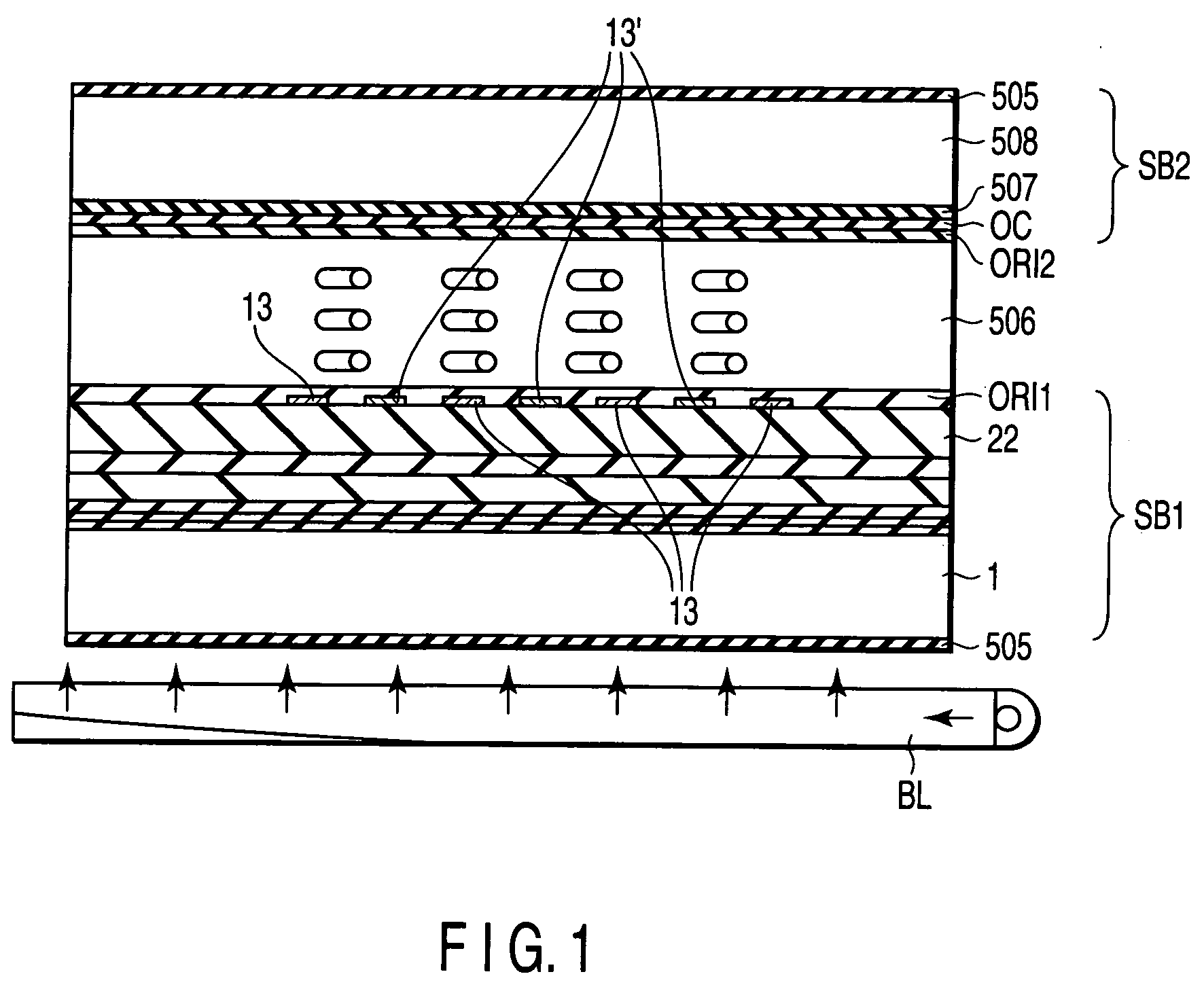
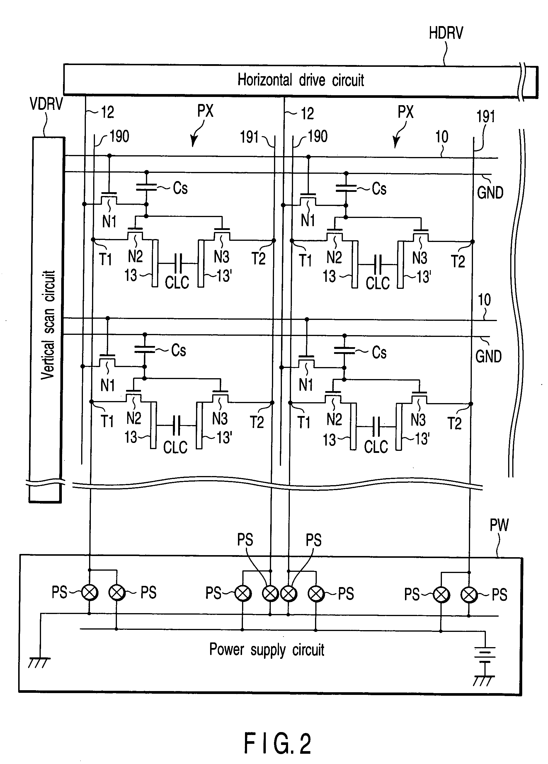
[0047]FIG. 1 shows the cross-sectional structure of the transmission-type active matrix liquid crystal display. FIG. 2 schematically shows the plan-view structure of this liquid crystal display. FIG. 3 shows an equivalent circuit of one of the pixel circuits PX that are arrayed in a matrix in the liquid crystal display shown in FIG. 2.

[0048] The liquid crystal display is configured such that a liquid crystal layer 506, for example, is held between a pair of support substrates SB1 and SB2, as shown in FIG. 1. The support substrate SB1 is formed by stacking a protection insulation film 22, etc. on a glass substrate 1. As shown in FIG. 2, the support substrate SB1 includes a plurality of pixel circuits PX arrayed in a matrix; a plurality of scan lines 10 arranged along the rows of pixel circuits PX; ...

second embodiment

[0093] A reflection-type active matrix liquid crystal display according to a second embodiment of the present invention will now be described. FIG. 11 shows the plan-view structure of a pixel circuit PX of the reflection-type active matrix liquid crystal display, and FIG. 12 shows the cross-sectional structure of the pixel circuit PX, taken along line B-B′ in FIG. 11.

[0094] This liquid crystal display is substantially the same as the liquid crystal display of the first embodiment, except for the electrode structure for reflecting ambient light. In FIG. 11 and FIG. 12, the parts similar to those in the first embodiment are denoted by the same reference numerals, and a detailed description of, e.g. film materials and stacked structures is omitted.

[0095] This liquid crystal display has the same circuit configuration as has been described with reference to FIG. 2 and FIG. 3. The first pixel electrode 13 and the second pixel electrode 13′ of the first embodiment, however, are replaced ...

third embodiment

[0097] A semi-transmission-type (“transflective”) active matrix liquid crystal display according to a third embodiment of the present invention will now be described. FIG. 13 shows the plan-view structure of a pixel circuit PX of the semi-transmission-type active matrix liquid crystal display, and FIG. 14 shows the cross-sectional structure of the liquid crystal display, taken along line B-B′ in FIG. 13. This liquid crystal display is substantially the same as the liquid crystal display of the first embodiment, except for the electrode structure for transmitting backlight and reflecting ambient light. In FIG. 13 and FIG. 14, the parts similar to those in the first embodiment are denoted by the same reference numerals, and a detailed description of, e.g. film materials and stacked structures is omitted.

[0098] The liquid crystal display has the circuit configuration that is described with reference to FIG. 2 and FIG. 3. A reflective electrode 150, however, is provided in addition to ...


PUM


Abstract

A liquid crystal display includes a pair of support substrates, a liquid crystal layer held between the substrates, and pixel circuits that are arrayed in a matrix on one of the substrates and control the alignment state of liquid crystal molecules. Each pixel circuit includes first and second power terminals, first and second pixel electrodes that apply a liquid crystal drive voltage to the liquid crystal layer to create a substantially lateral electric field, and first and second drive transistors that have gate electrodes for receiving a video signal, that are connected between the first power terminal and the first pixel electrode and between the second power terminal and the second pixel electrode, respectively, and that cause the liquid crystal drive voltage determined by conductances that vary in accordance with the video signal, to be retained in a liquid crystal capacitance between the first and second pixel electrodes.

Description

CROSS-REFERENCE TO RELATED APPLICATIONS [0001] This application is based upon and claims the benefit of priority from prior Japanese Patent Application No. 2004-032440, filed Feb. 9, 2004, the entire contents of which are incorporated herein by reference. BACKGROUND OF THE INVENTION [0002] 1. Field of the Invention [0003] The present invention relates to a liquid crystal pixel memory, a liquid crystal display, and methods of driving the liquid crystal pixel memory and the liquid crystal display, wherein a liquid crystal drive voltage, the polarity of which is cyclically reversed in order to control the alignment state of liquid crystal molecules, is applied to a liquid crystal layer. [0004] 2. Description of the Related Art [0005] An active matrix liquid crystal display, for example, is used in OA apparatuses or other various apparatuses as a display device for displaying information such as characters and graphics. This liquid crystal display is a display panel that has, in usual c...

Claims


Application Information

Patent Timeline
Patent Type & Authority Applications(United States)
IPC IPC(8): G09G3/20G09G3/36
CPCG09G3/2011G09G3/3614G09G3/3655G09G2300/0876G09G2300/0814G09G2300/0823G09G2300/0456
Inventor KAWACHI, GENSHIRO
Owner ADVANCED LCD TECH DEVMENT CENT
Why Eureka
Try Eureka