Organic light-emitting device having thin-film encapsulation portion, method of manufacturing the device, and apparatus for forming a film

Inactive Publication Date: 2005-08-18
SAMSUNG MOBILE DISPLAY CO LTD
View PDF15 Cites 90 Cited by
  • Summary
  • Abstract
  • Description
  • Claims
  • Application Information

AI Technical Summary

Benefits of technology

[0018] It is still an object of the present invention to provide a design for an OLED having an encapsulating layer that prevents moisture from reaching the organic layer while being transparent to visible light.
[0019] It is further an object of the present invention to provide a design for an OLED that is flexible or bendable while protecting the organic layer from moisture.
[0020] It is further an object of the present invention to provide a method for making and apparatus for making the novel OLED that leads to low production costs.
[0021] It is also an object of the pres

Problems solved by technology

However, when manufacturing flat panel displays, the formation of organic layers, a TFT layer, electrode layers, or an orientation layer, etc. for flat panel displays is difficult, complex and expensive.
However, in the above organic light-emitting device, the organic thin layers are separately produced, and thus cannot be easily aligned at the time of connecting both waterproof films.
In addition, the attachment of an organic layer having a specific pattern may not be increased.
However, the use of this structure in front emission type devices is limiting since light is emitted in an opposite direction to the substrate on which an organic layer is formed, i.e., in a direction toward the encapsulation structure in the front emission type devices.
The thin-film encapsulation structure described above cannot efficiently protect the light producing organic layer from moisture or air.
However, the organic layer may be adversely affected by the production process

Method used


Image

  • Organic light-emitting device having thin-film encapsulation portion, method of manufacturing the device, and apparatus for forming a film
  • Organic light-emitting device having thin-film encapsulation portion, method of manufacturing the device, and apparatus for forming a film
  • Organic light-emitting device having thin-film encapsulation portion, method of manufacturing the device, and apparatus for forming a film

Examples


Embodiment Construction

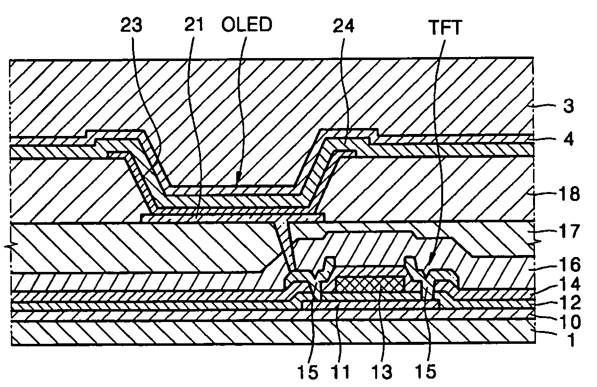
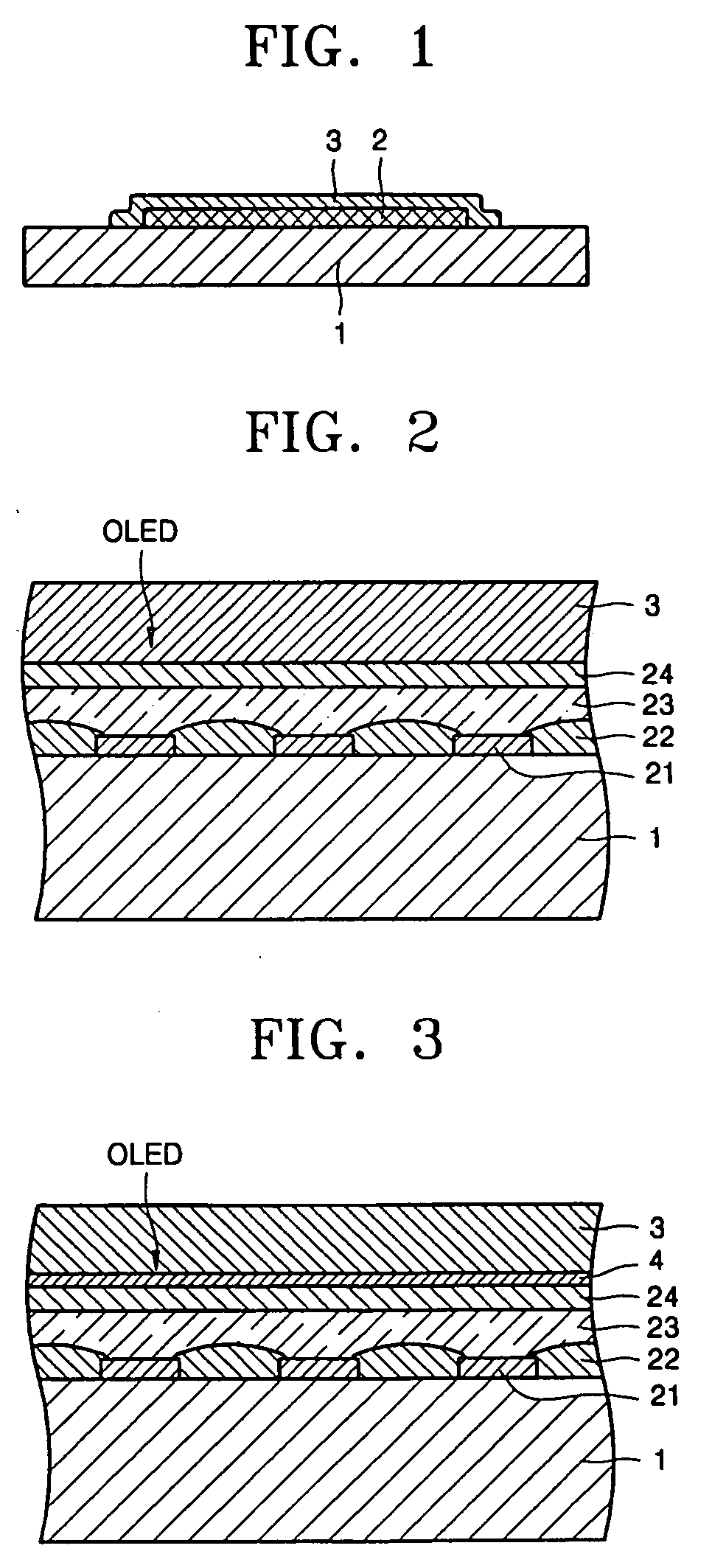
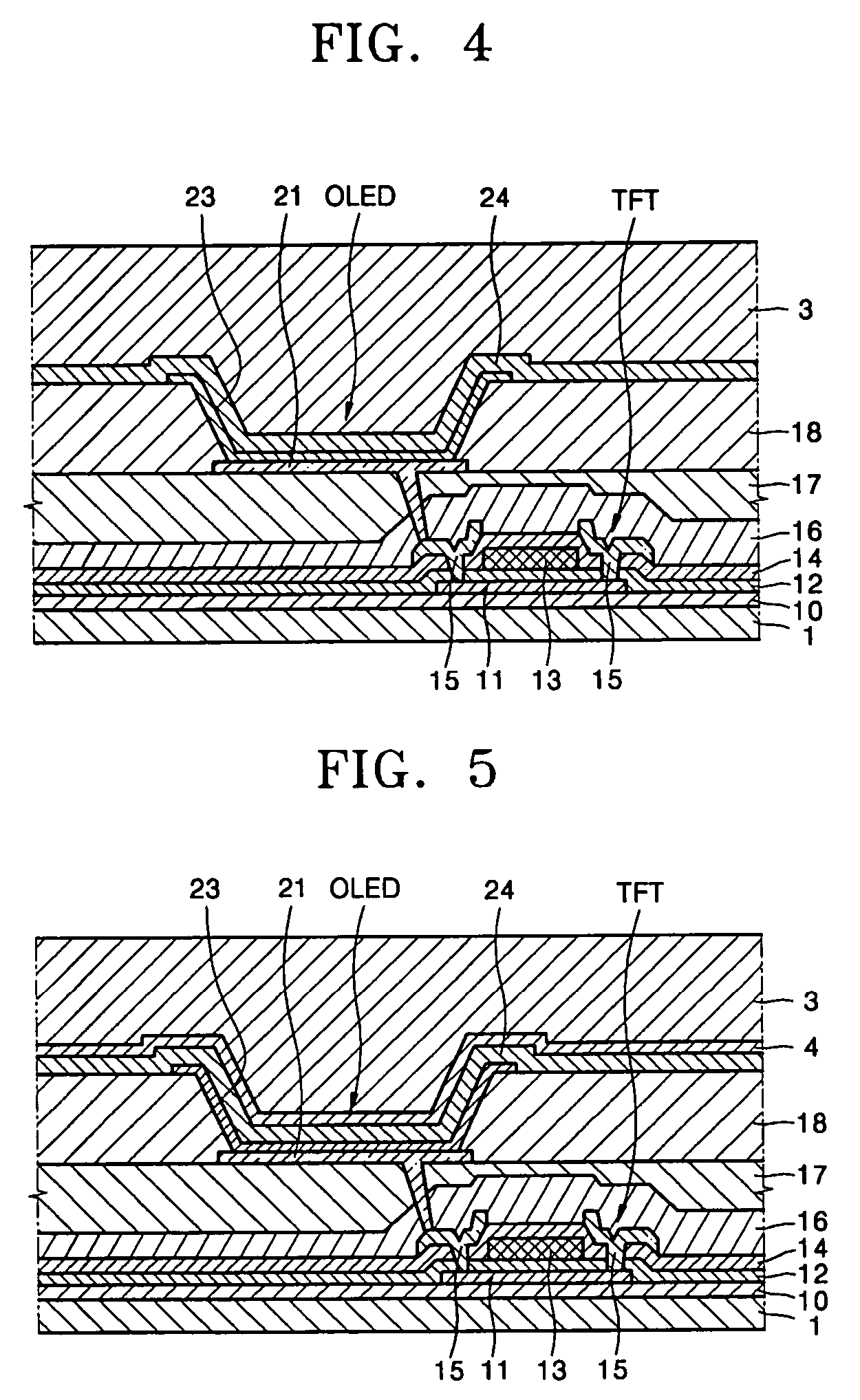
[0039] Turning now to the figures, FIG. 1 is a cross-sectional view of an ultra-thin organic light-emitting device according to an embodiment of the present invention. Referring to FIG. 1, the ultra-thin organic light-emitting device includes a substrate 1, an organic light-emitting portion 2 including an organic light-emitting diode (OLED) formed on a surface of the substrate 1, and an encapsulation portion 3 formed to encapsulate the organic light-emitting portion 2. The substrate 1 may be made of a transparent glass. The substrate 1 may also be made of flexible plastics or metals. A buffer layer may be formed on the top surface of the substrate 1.

[0040] The organic light-emitting portion 2 includes the OLED and realizes a predetermined image. Various types of OLEDs may be used in the organic light-emitting portion 2. That is, any one of a passive matrix (PM) type OLED, that is simple matrix type, and an active matrix (AM) type OLED, that includes a thin film transistor (TFT) lay...


PUM


Abstract

An organic light-emitting device that includes an encapsulation structure that has excellent resistance to water, heat, and chemicals and can be mass-produced, a method of manufacturing the device, and an apparatus for manufacturing the encapsulation structure. The organic light-emitting device includes a substrate, an organic light-emitting portion that has an organic light-emitting diode (OLED) and formed on a surface of the substrate, and an encapsulation structure made of a parylene polymer and formed to cover the organic light-emitting portion.

Description

CLAIM OF PRIORITY [0001] This application makes reference to, incorporates the same herein, and claims all benefits accruing under 35 U.S.C. §119 from an application for ORGANIC LIGHT-EMITTING DEVICE HAVING THIN-FILM ENCAPSULATION PORTION, METHOD OF MANUFACTURING THE DEVICE, AND APPARATUS FOR FORMING A FILM earlier filed in the Korean Intellectual Property Office on 17 Feb. 2004 and there duly assigned Serial No. 2004-10415. BACKGROUND OF THE INVENTION [0002] 1. Field of the Invention [0003] The present invention relates to an organic light-emitting device having a thin-film encapsulation portion, a method of manufacturing the device, and an apparatus for forming the encapsulation portion, and more particularly, to an organic light-emitting device having an encapsulation portion made of a parylene polymer, a method of manufacturing the device, and an apparatus for making the parylene polymer film. [0004] 2. Description of the Related Art [0005] Generally, flat panel displays, such a...

Claims


Application Information

Patent Timeline
IPC IPC(8): H01L27/32H01L51/50H05B33/04H01L51/52H05B33/10H05B33/14
CPCH01L27/3244H05B33/04H01L2251/5315H01L51/5237H10K59/12H10K50/844H10K2102/3026B60C19/122
Inventor KIM, HAN-KI
Owner SAMSUNG MOBILE DISPLAY CO LTD
Why Eureka
Try Eureka