Configurable prober for TFT LCD array testing

a prober and configuration technology, applied in the field of electric beam testing systems, can solve the problem of high cost of individual probers for new device layouts

Active Publication Date: 2005-08-18
APPLIED MATERIALS INC
View PDF99 Cites 32 Cited by
  • Summary
  • Abstract
  • Description
  • Claims
  • Application Information

AI Technical Summary

Benefits of technology

[0015] In one arrangement, the prober bars are “y” bars, and the configurable prober further includes at least one “x” prober bar. The “x” bar is attached along the “y” axis of the frame orthogonal to the “y” axis. A first end of the “x” prober bar is releasably connected to the frame, and a second end of the “x” prober bar is releasably connected to one of the at least one “y” prober bars. In this arrangement, each of the “y” prober bars may have a bar connection mechanism that allows for ready relocation of the at least one “x” prober bar to the “y” prober bar at selected points along the “y” prober bar.

Problems solved by technology

Modification of an individual prober for a new device layout is expensive.

Method used


Image

  • Configurable prober for TFT LCD array testing
  • Configurable prober for TFT LCD array testing
  • Configurable prober for TFT LCD array testing

Examples


Embodiment Construction

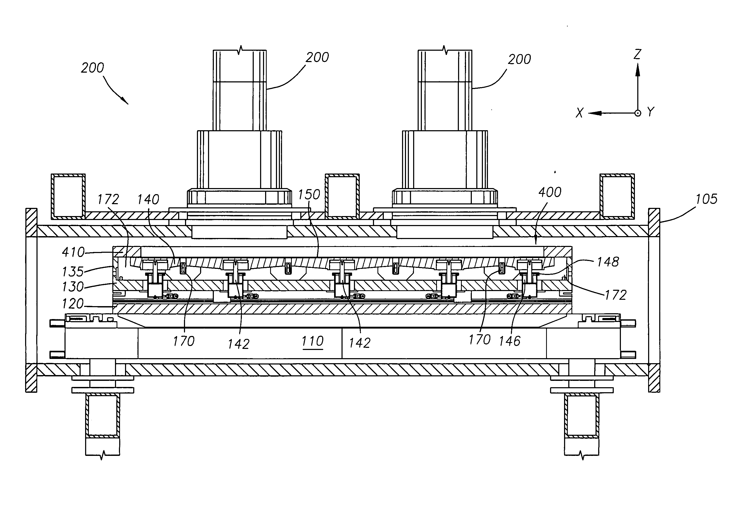
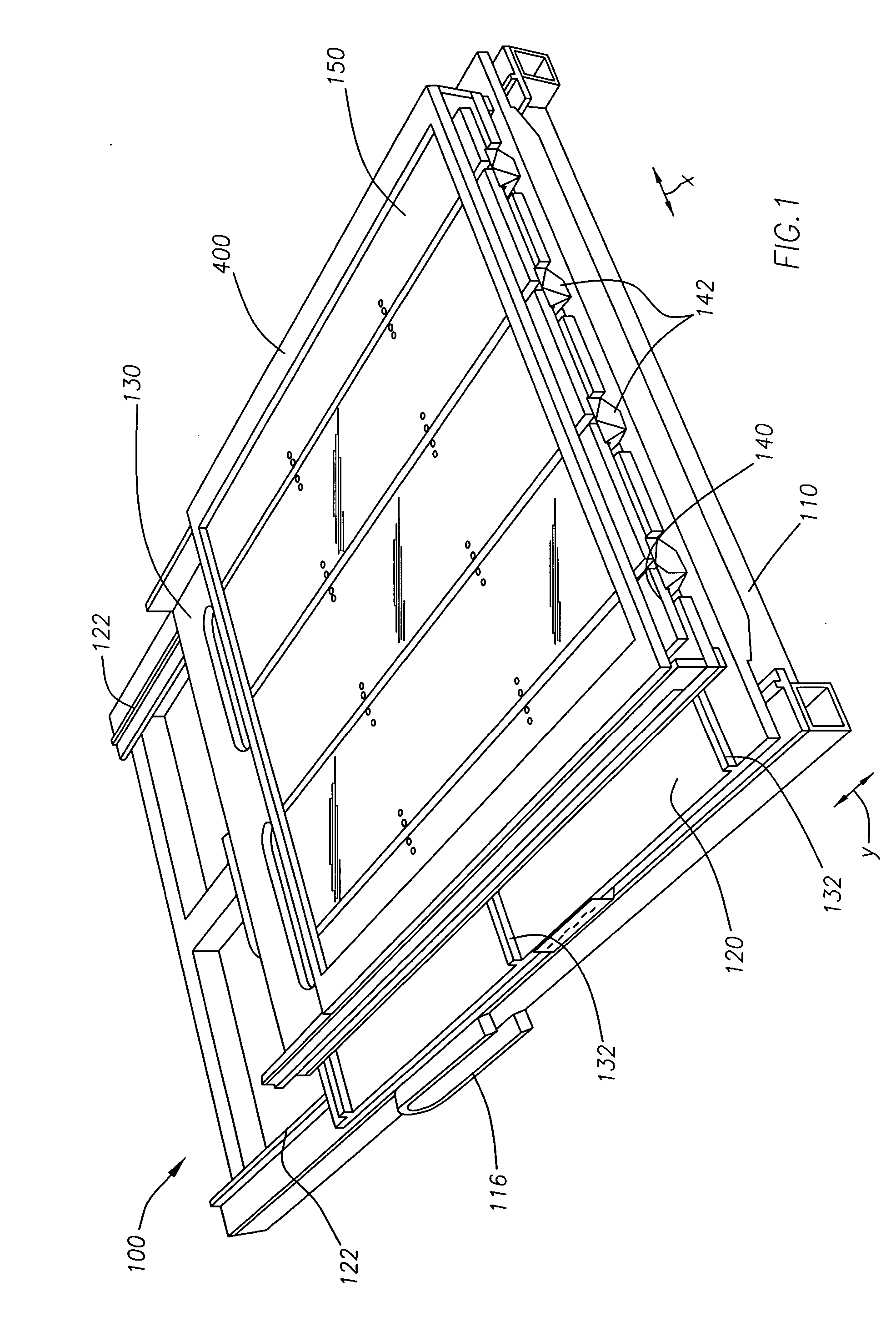
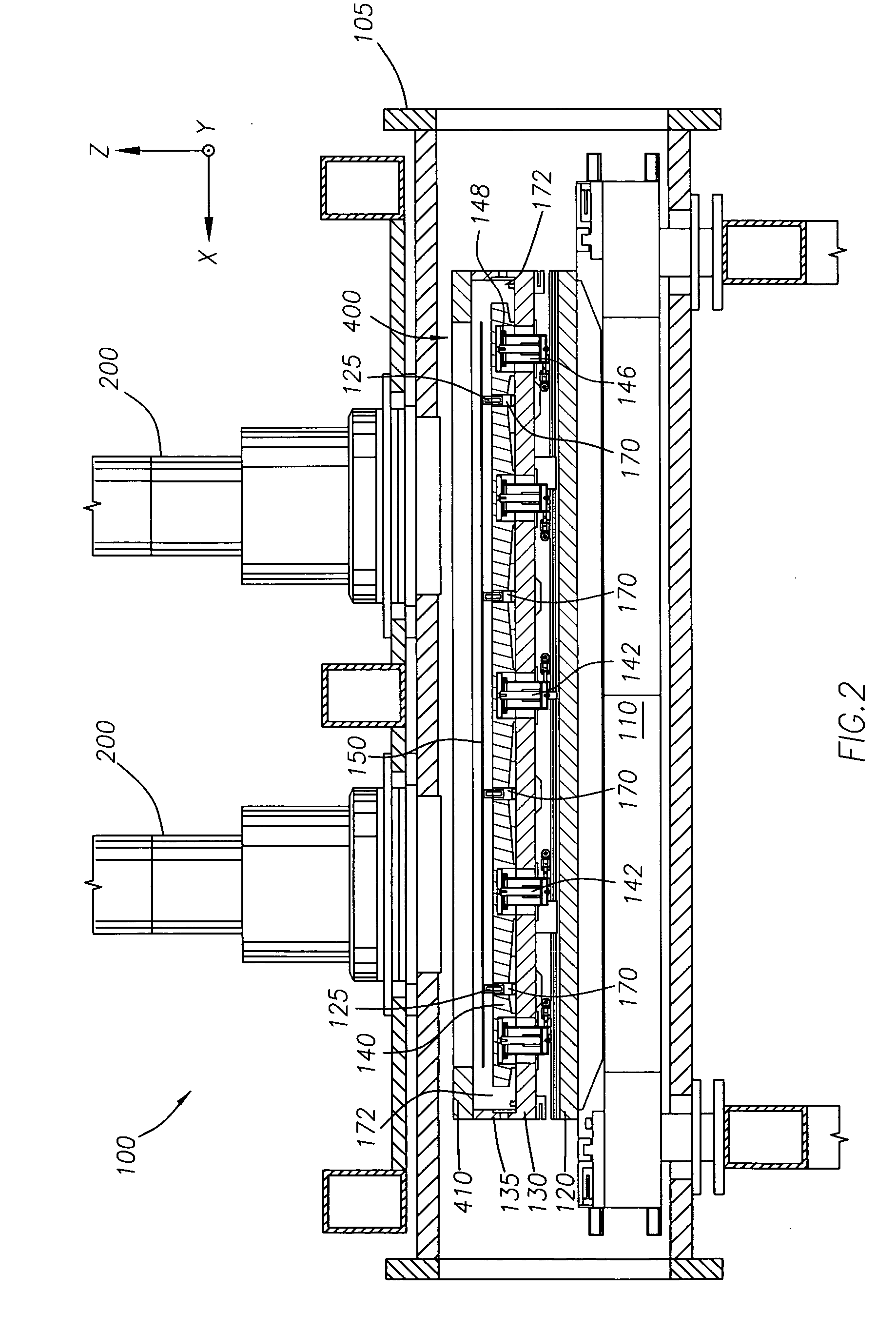
[0026] The present invention generally provides an improved prober for an electronic devices test system. For purposes of this disclosure, the term “test system” means any system that may be used to test electronic devices on a substrate. Such a test system may include optical inspection systems, electron beam test systems, systems that detect color changes, and others. The prober for the electronic devices test system is “configurable,” meaning that it can be adapted for different device layouts and substrate sizes.

[0027]FIG. 1 presents a perspective view of a configurable prober 400, in one embodiment. The prober 400 is part of an electronics device test system 100. In one embodiment, the prober 400 is part of an electron beam test system 100, though other systems could be used. The prober 400 is positioned on a test system table 110 that moves the prober 400 in at least “x” and “y” directions. In the arrangement of FIG. 1, the table 110 defines a tubular frame fabricated from st...


PUM

PropertyMeasurementUnit
areaaaaaaaaaaa
lengthaaaaaaaaaa
electron beam testingaaaaaaaaaa

Abstract

An improved prober for an electronic devices test system is provided. The prober is “configurable,” meaning that it can be adapted for different device layouts and substrate sizes. The prober generally includes a frame, at least one prober bar having a first end and a second end, a frame connection mechanism that allows for ready relocation of the prober bar to the frame at selected points along the frame, and a plurality of electrical contact pins along the prober bar for placing selected electronic devices in electrical communication with a system controller during testing. In one embodiment, the prober is be used to test devices such as thin film transistors on a glass substrate. Typically, the glass substrate is square, and the frame is also square. In this way, “x” and “y” axes are defined by the frame.

Description

CROSS-REFERENCE TO RELATED APPLICATIONS [0001] This application is a continuation-in-part of co-pending U.S. patent application Ser. No. 10 / 778,982, filed Feb. 12, 2004. That application is entitled “Electron Beam Test System with Integrated Substrate Transfer Module.” That application is incorporated herein in its entirety by reference.BACKGROUND OF THE INVENTION [0002] 1. Field of the Invention [0003] Embodiments of the present invention generally relate to electron beam testing systems for semiconductor devices on substrates. More particularly, embodiments of the present invention generally relate to an improved prober for conducting a thin film transistor liquid crystal display array test on a variety of glass panel substrate designs. [0004] 2. Description of the Related Art [0005] Active matrix liquid crystal displays (LCDs) are commonly used for applications such as computer and television monitors, cell phone displays, personal digital assistants (PDAs), and an increasing num...

Claims


Application Information

Patent Timeline
Patent Type & Authority Applications(United States)
IPC IPC(8): G01R31/26G01R31/302G01R31/305G02F1/13G09G3/00H01L21/687
CPCG01R31/2893G09G3/006G01R31/305
Inventor BRUNNER, MATTHIASKURITA, SHINICHISCHMID, RALFABBOUD, FAYEZ FRANK E.JOHNSTON, BENJAMINBOCIAN, PAULBEER, EMANUEL
Owner APPLIED MATERIALS INC
Why Eureka
Try Eureka