Multiband antenna suitable for miniaturization

a multi-band antenna and miniaturization technology, applied in the field of multi-band antennas, can solve the problems of high cost, complex circuit structure, and difficulty in implementing small size, and achieve the effect of low cost and simplified circuit structur

Inactive Publication Date: 2005-08-18
ALPS ALPINE CO LTD
View PDF5 Cites 29 Cited by
  • Summary
  • Abstract
  • Description
  • Claims
  • Application Information

AI Technical Summary

Benefits of technology

[0010] Accordingly, the present invention has been made to solve the above-mentioned problems and it is an object of the present invention to provide a multiband antenna capable of simplifying a circuit structure while maintaining a small size and reducing a manufacturing cost.
[0012] In the multiband antenna having the above-mentioned structure, since an interval between an inner circumferential portion serving as a shorting portion of the second radiating conductor and an outer circumferential portion of the first radiating conductor is made to be small so that both radiating conductors may be substantially electromagnetically coupled with each other, when the first radiating conductor is excited at a frequency fH by direct power feeding, the second radiating conductor may be excited at a frequency fL lower than the frequency fH. In addition, when a third radiating conductor is disposed at a location which surrounds the second radiating conductor to make both radiating conductors substantially electromagnetically coupled with each other, the third radiating conductor may also be excited at a frequency much lower than the frequency fL. That is, the multiband antenna may allow several kinds of radiating conductors concentrically disposed on the same plane to be excited at different frequencies from each other, which is suitable for implementation of the small size, and separate power feeding is not required, so that the circuit structure may be simplified.
[0015] In addition, in the multiband antenna having the above-mentioned structure, the first and second radiating conductors are provided on one surface of the dielectric substrate, and the grounding conductor is provided on the other surface of the dielectric substrate, so that the antenna may be simply fabricated with low cost. In this case, the first and second radiating conductors may be collectively formed on one surface of one sheet of a dielectric substrate while the height of the antenna may be suppressed to about a thickness of the dielectric substrate.
[0016] In addition, in the multiband antenna having the above-mentioned structure, the first and second radiating conductors are metal plates, and a metal piece extending from a power feeding point of the first radiating conductor toward the grounding conductor acts to a feeding pin which is isolated from the grounding conductor, and a metal piece extending from the inner circumferential portion of the second radiating conductor toward the grounding conductor is shorted from the grounding conductor, so that the antenna may be simply fabricated with low cost. In this case, all of the first and second radiating conductors, a feeding pins and a shorting means such as a shorting pins or the like may be formed from one sheet of metal plate and the dielectric substrate may be even omitted, so that the fabrication cost may significantly decrease.
[0018] According to the dualband antenna of the present invention, when the inner circumferential portion of the second radiating conductor which surrounds the first radiating conductor is shorted from the grounding conductor and the first radiating conductor is excited by direct power feeding, the second radiating conductor is configured to excite at a different frequency by means of the electromagnetic coupling, it is possible to use a plurality of types of resonance frequency while maintaining the small-sized antenna. In addition, separate power feeding is not required, so that the circuit structure may be simplified, which readily leads to the implementation of low cost.

Problems solved by technology

However, since a large space is required to separately mount the antenna for ETC and the antenna for GPS and the mounting work is complicated, multiband antennas capable of using several kinds of resonance frequencies have generally been proposed.
As a result, there is a problem in that the circuit structure is complicated and the high cost is required.
However, the latter conventional example has a structure where two sheets of dielectric substrates are laminated, so that it is difficult to implement the small size and hard to say that it is effective in cost because two metallic moulds for the dielectric substrates are required.

Method used


Image

  • Multiband antenna suitable for miniaturization
  • Multiband antenna suitable for miniaturization
  • Multiband antenna suitable for miniaturization

Examples


first embodiment

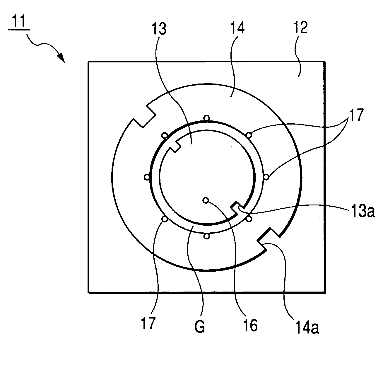
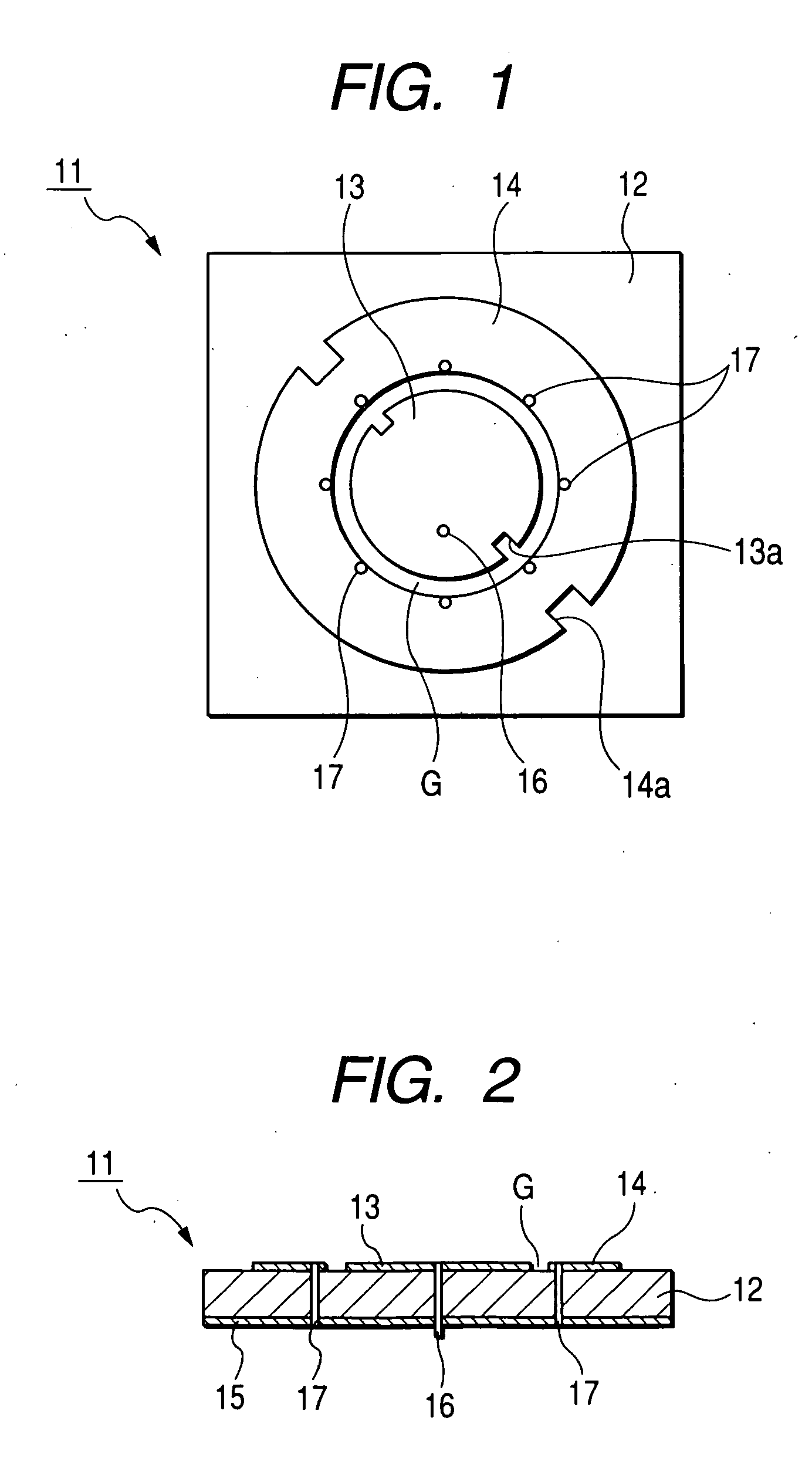
[0027] Preferred embodiments of the present invention will be described with reference to the accompanying drawings. FIG. 1 shows a plan view of a circularly polarized wave antenna for dualband according to the present invention, and FIG. 2 shows a cross-sectional view of the circularly polarized wave antenna for dualband.

[0028] In the circularly polarized wave antenna 11 for dualband shown in the drawings, a first radiating conductor 13 for high band and a second radiating conductor 14 for low band are concentrically formed on a top surface of a dielectric substrate 12, and a grounding conductor 15 is formed over a substantially entire surface of a bottom surface of the dielectric substrate 12. The first radiating conductor 13 is circular, and cut-shaped degeneracy isolation elements 13a are provided at two locations of an outer circumferential portion of the first radiating conductor 13 which face each other. The second radiating conductor 14 having an annular shape is disposed at...

third embodiment

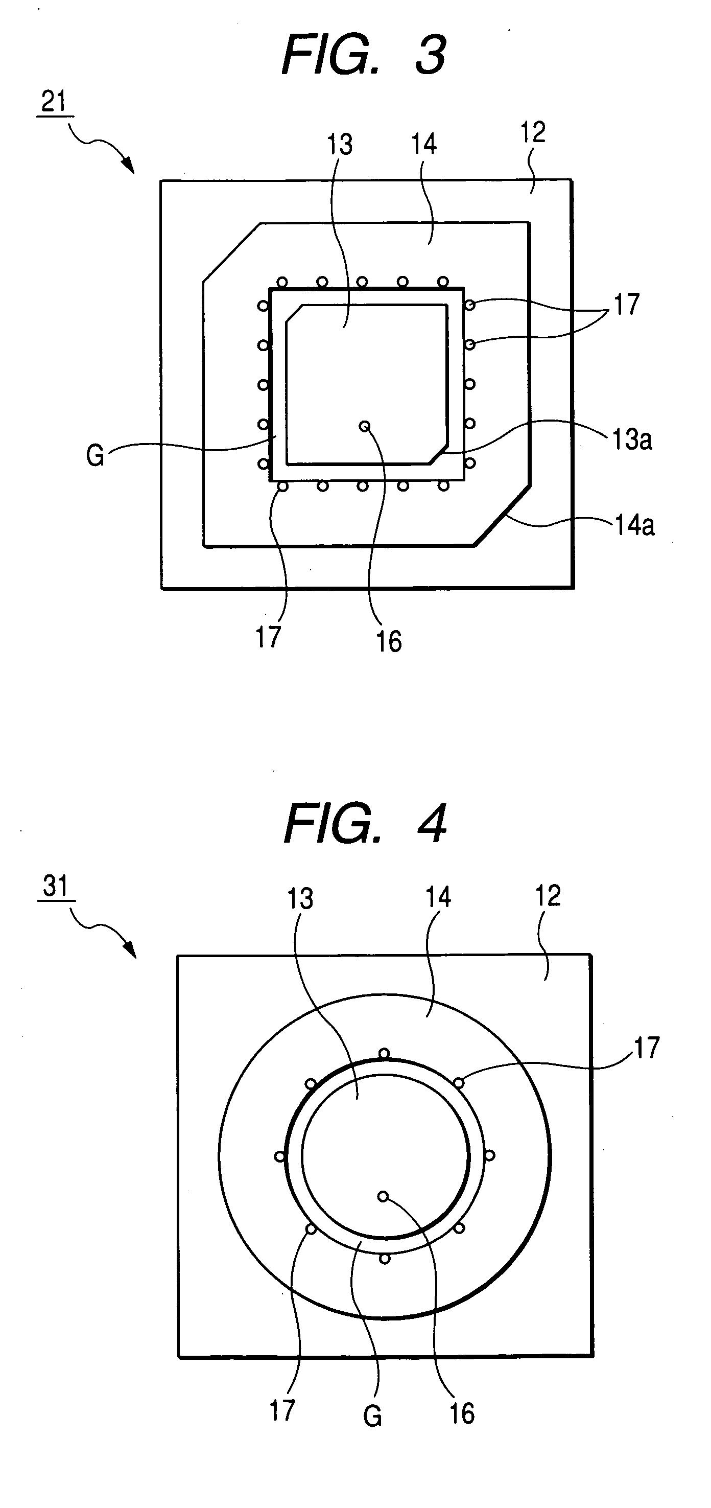
[0033]FIG. 4 is a plan view of a linearly polarized wave antenna for dualband according to the present invention, and has the same reference numerals as those given to the corresponding parts of FIG. 1. A dualband antenna 31 shown in FIG. 4 allows the first and second radiating conductors 13 and 14 electromagnetically coupled with each other to be excited with linearly polarized waves at different frequencies from each other. Therefore, the radiating conductors 13 and 14 are formed such that the degeneracy isolation elements are not provided, that is, the first radiating conductor 13 is formed to be circular and the second radiating conductor 14 is formed to be annular. Alternatively, the first radiating conductor 13 may be formed to be square and the second radiating conductor 14 may be formed to be rectangular.

fourth embodiment

[0034]FIG. 5 is a plan view of a linearly polarized wave antenna for dualband according to the present invention, and FIG. 6 is a cross-sectional view of the linearly polarized wave antenna for dualband, where a reference numeral 18 indicates a grounding conductor plate and parts corresponding to FIGS. 1 to 4 are denoted by the same reference numerals. The dualband antenna 41 shown in FIGS. 5 and 6 is a metal plate antenna from which the dielectric substrate is removed, and one sheet of metal plate is used to form all of the first and second radiating conductors 13 and 14, the feeding pin 16, and the shorting pin 17. In other words, the first radiating conductor 13 is a circular metal plate, wherein a metal piece (a cut and erected piece) extending from its feeding point toward the grounding conductor plate 18 serves as the feeding pin 16 away from the grounding conductor plate 18, and the first radiating conductor 13 is supported by the feeding pin 16 above the grounding conductor ...


PUM


Abstract

First and second radiating conductors are concentrically formed on a top surface of a dielectric substrate, and a grounding conductor is formed on a bottom surface of the dielectric substrate. A feeding pin is connected to a power feeding point of the first radiating conductor. Shorting pins are connected to an inner circumferential portion of the second radiating conductor to be shorted by the grounding conductor. An interval between the radiating conductors allows the first and second radiating conductors to be electromagnetically coupled with each other. When the first radiating conductor is excited at a frequency fH by direct feeding from the feeding pin, the second radiating conductor is fed by the coupling, so that it is excited at a frequency fL lower than the frequency fH.

Description

BACKGROUND OF THE INVENTION [0001] 1. Field of the Invention [0002] The present invention relates to a multiband antenna capable of using a plurality of kinds (for example, two kinds) of resonance frequencies, and more particular, to a small-sized multiband antenna suitable for a vehicle or the like. [0003] 2. Description of the Related Art [0004] Recently, automobiles which have mounted an antenna for electronic toll collection system (ETC) having an operation frequency of a 5.8 GHz band or an antenna for global positioning system (GPS) having an operation frequency of a 1.5 GHz band are rapidly increasing. However, since a large space is required to separately mount the antenna for ETC and the antenna for GPS and the mounting work is complicated, multiband antennas capable of using several kinds of resonance frequencies have generally been proposed. [0005] As an example of such a multiband antenna, a structure of a patch antenna has been well known in a conventional art as shown i...

Claims


Application Information

Patent Timeline
Patent Type & Authority Applications(United States)
IPC IPC(8): H01Q21/30H01Q1/38H01Q5/10H01Q5/378H01Q9/04H01Q13/08H01Q21/28
CPCH01Q1/38H01Q9/0407H01Q5/378H01Q21/28H01Q9/0464
Inventor HIGASA, MASAHIKOSHIKATA, MASARU
Owner ALPS ALPINE CO LTD
Why Eureka
Try Eureka