System for improving thermal stability of copper damascene structure

a technology of damascene and thermal stability, which is applied in the direction of semiconductor/solid-state device manufacturing, basic electric elements, electric devices, etc., can solve the problems of device failure, copper is very difficult to etch in the semiconductor process flow, circuit generates numerous challenges to the semiconductor manufacturing process, etc., and achieves the effect of adding excessive costs or procedures and being more reliabl

Inactive Publication Date: 2005-08-25
LU JIONG PING +5
View PDF11 Cites 5 Cited by
  • Summary
  • Abstract
  • Description
  • Claims
  • Application Information

AI Technical Summary

Benefits of technology

[0009] As should now be apparent, a method of forming copper interconnect structures that does not add excessive costs or procedures to the fabrication process is now needed, providing for fabrication of more reliable semiconductor devices while overcoming the aforementioned limitations of conventional methods.

Problems solved by technology

The increased packing density of the integrated circuit generates numerous challenges to the semiconductor manufacturing process.
Unfortunately, copper is very difficult to etch in a semiconductor process flow.
During anneal steps, deposited copper interconnects frequently form voids at via bottoms and other interfaces, which may ultimately cause device failure.
A low temperature anneal, however, will not completely stabilize the deposited copper and also result in device failure.
Stresses within the copper interconnect structure may cause the interconnect to fail during the high temperature annealing process, which also causes via open failures.

Method used


Image

  • System for improving thermal stability of copper damascene structure
  • System for improving thermal stability of copper damascene structure
  • System for improving thermal stability of copper damascene structure

Examples


Embodiment Construction

[0016] It should be understood that the principles and applications disclosed herein may be applied to a wide range of semiconductor device fabrication processes. For purposes of explanation and illustration, the present invention is hereafter described in reference to several specific embodiments of methods of semiconductor device fabrication. The present invention, however, is equally applicable in any number of fabrication processes that might benefit from the present invention.

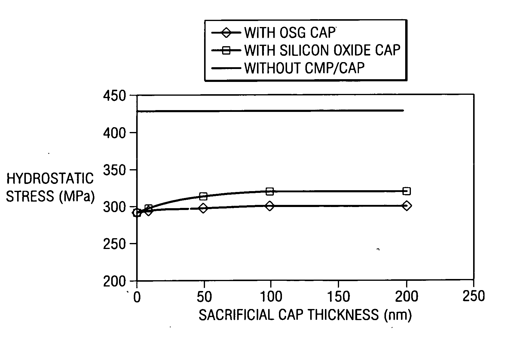
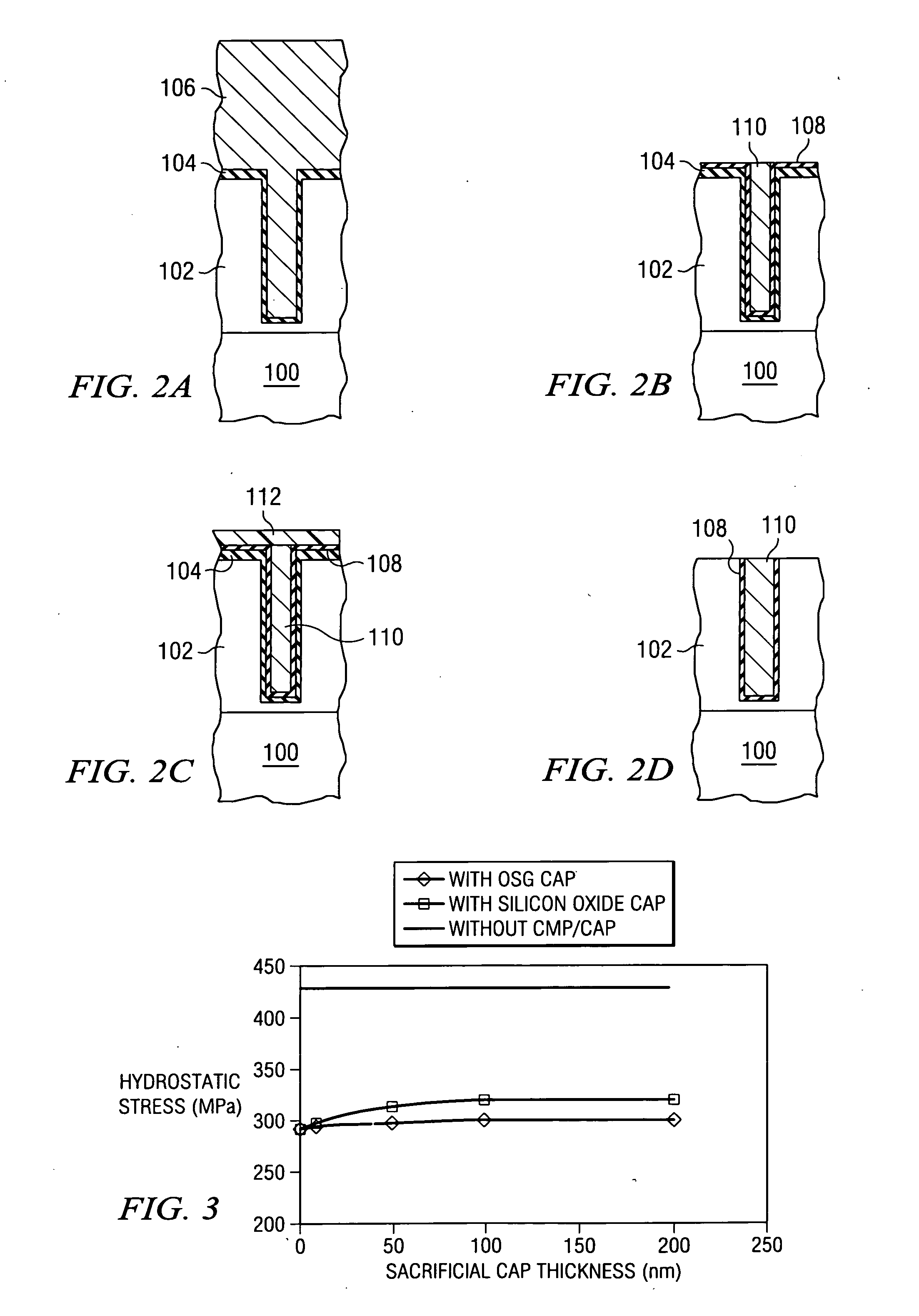
[0017] Turning now to the present invention as depicted in FIGS. 2A-2D, a copper interconnect structure may be formed, for example, generally according to the procedures depicted in and described with reference to FIGS. 1A-1D above. As depicted in FIG. 2A, the interlevel dielectric 102 is formed over the semiconductor body 100. The interlevel dielectric 102 is then patterned and etched to remove the dielectric material from the areas 118 (not shown) where interconnect lines are desired. The barrier layer ...


PUM


Abstract

Disclosed is a system for fabricating a semiconductor device (100). An interconnect structure (110) is formed on the semiconductor device (100) and a cap (112) is deposited over the interconnect structure (110). The interconnect structure (110) is annealed with the overlying cap (112) in place. The cap (112) is then removed after the interconnect structure (110) is annealed.

Description

FIELD OF THE INVENTION [0001] The invention is related generally to the field of fabricating interconnect structures for integrated circuits and, more specifically, to improving the thermal stability of copper damascene interconnect structures. BACKGROUND OF THE INVENTION [0002] This application claims priority from Provisional Application Ser. No. 60 / 344,465, filed on Dec. 28, 2001. [0003] Since the invention of integrated circuits, the number of devices on a chip has grown at a near-exponential rate. The fabrication methods of the semiconductor industry have been modified and improved continuously for almost four decades. With each improved method, the capacity of a single semiconductor chip has increased from several thousand devices to hundreds of million devices. Future improvements will require integrated circuit devices such as transistors, capacitors, and connections between devices to become even smaller and more densely populated on the chip. [0004] The increased packing d...

Claims


Application Information

Patent Timeline
Patent Type & Authority Applications(United States)
IPC IPC(8): H01L21/768
CPCH01L21/76834H01L21/76883H01L21/76877
Inventor LU, JIONG-PINGHONG, QI-ZHONGCHIU, TZ-CHENGJIN, CHANGMINGPERMANA, DAVIDTSUI, TING
Owner LU JIONG PING
Why Eureka
Try Eureka