Liquid crystal display and ESD protection circuit thereof

a protection circuit and liquid crystal display technology, applied in the direction of circuit arrangements, instruments, computing, etc., can solve the problems of damage to the display cell, damage to the lcd circuit, etc., and achieve the effect of reducing the influence of esd stress on the display cell

Active Publication Date: 2005-09-01
AU OPTRONICS CORP
View PDF7 Cites 33 Cited by
  • Summary
  • Abstract
  • Description
  • Claims
  • Application Information

AI Technical Summary

Benefits of technology

[0015] One object, among others, of the present invention is thus to provide a LCD protection circuit comprising a buffer circuit connected between the short ring and the common electrode to reduce the influence of ESD stress on the display cell.

Problems solved by technology

During manufacture of LCD panels, ESD frequently occurs on the isolated glass substrate and damages the LCD circuit.
During manufacture of LCD panels, however, ESD may occur on the common electrode 14 and damage the display cell 100 through the turned-on diode 18.
Thus, the conventional short ring cannot prevent the occurrence of ESD on the common electrode 14 and resulting damage to the display cell 100.
Additionally, the common electrode 14 is not grounded, and ESD protection provided thereby is limited.

Method used


Image

  • Liquid crystal display and ESD protection circuit thereof
  • Liquid crystal display and ESD protection circuit thereof
  • Liquid crystal display and ESD protection circuit thereof

Examples


Embodiment Construction

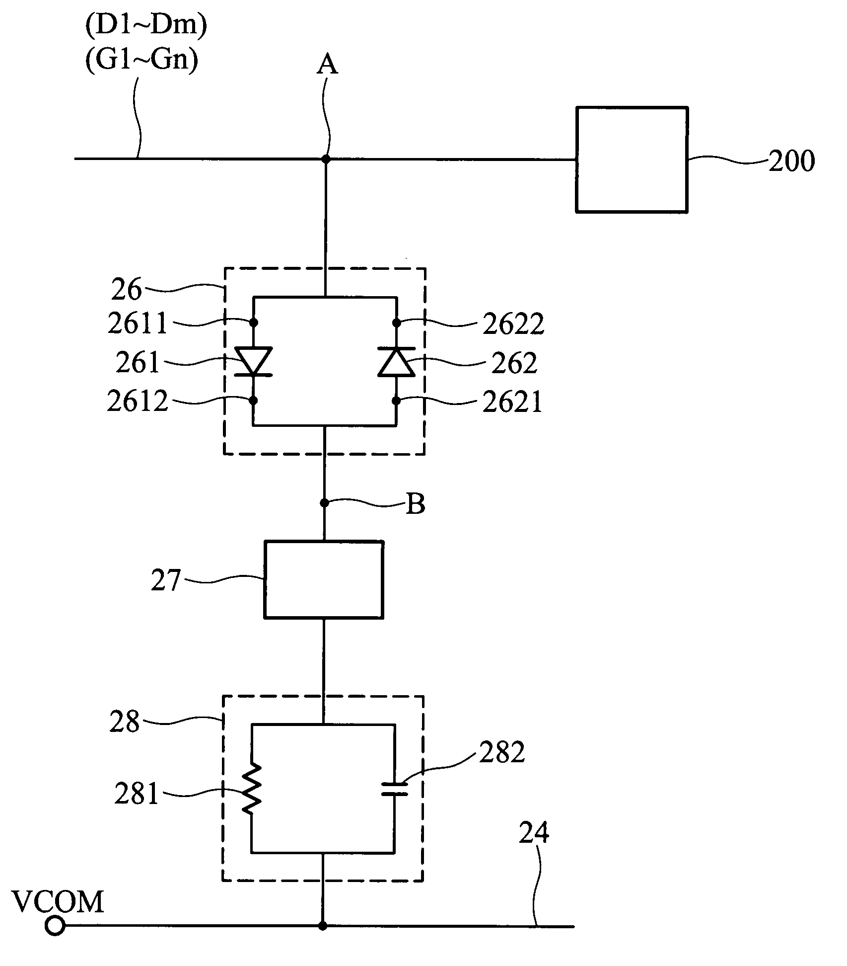
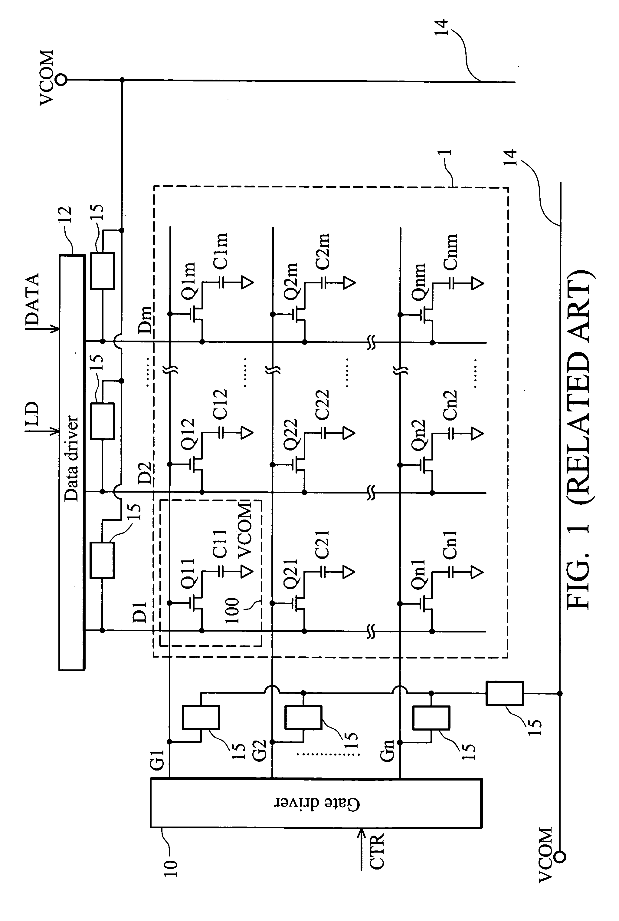
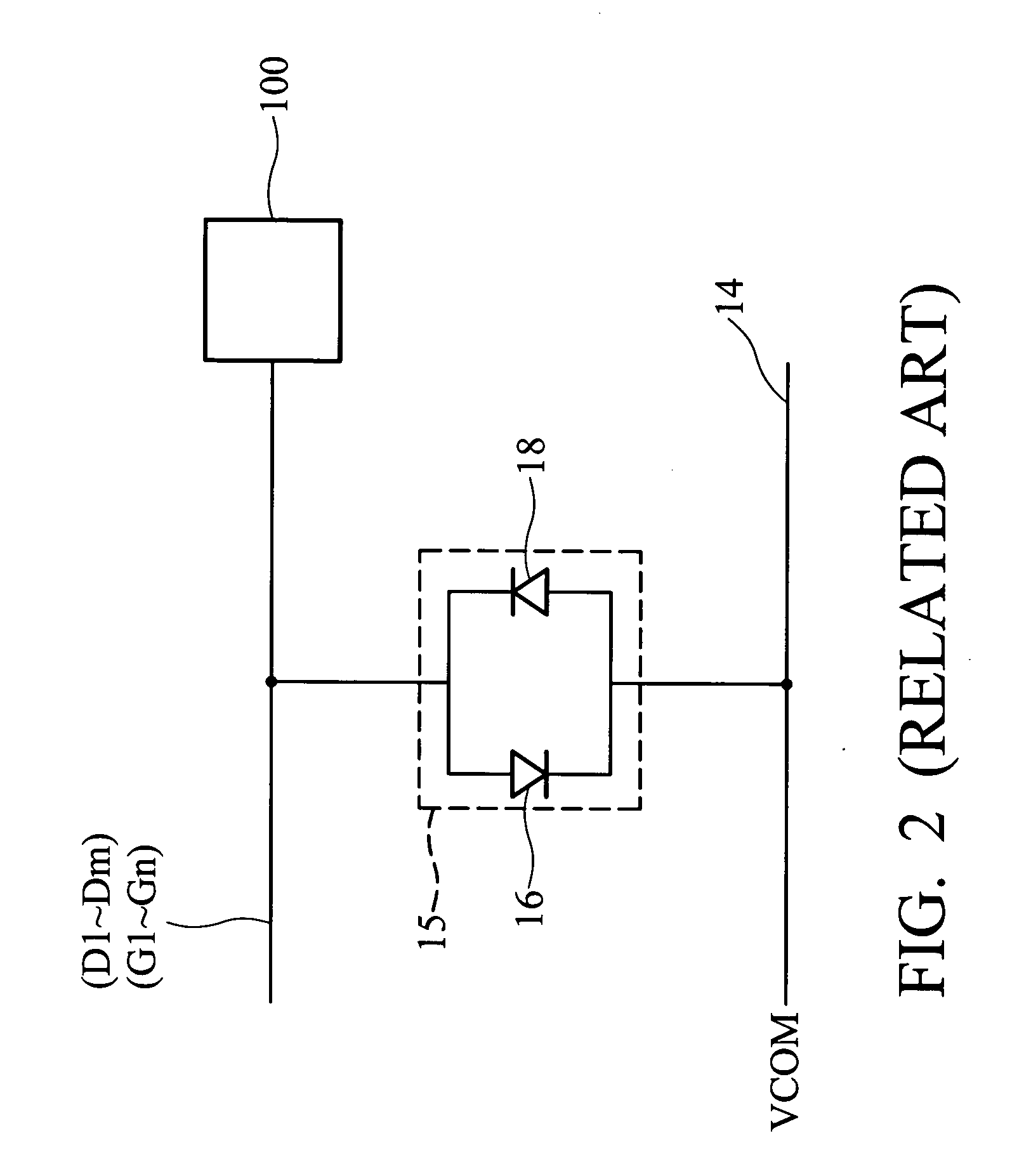
[0023]FIG. 3 is a schematic diagram of a conventional liquid crystal display panel and the peripheral driving circuits thereof. As shown in the figure, an LCD panel 3 is formed by interlacing data electrodes (represented by D1, D2, D3,. . . , Dm) and gate electrodes (represented by G1, G2, G3,. . . , Gm), each of the interlaced data electrodes and gate electrodes control a display cell. As an example, interlaced data electrode D1 and gate electrode G1 control the display cell 200. The equivalent circuit of each display cell comprises thin film transistors (TFTs) (Q11-Q1m, Q21-Q2m, . . . , Qn1-Qnm) and storage capacitors (C11-C1m, C21-C2m, . . . , Cn1-Cnm). The gates and drains of the TFTs are respectively connected to gate electrodes (G1-Gn) and data electrodes (D1-Dm). The connection can turn on / off all the TFTs on the same line (i.e. positioned on the same scan line) using a scan signal of gate electrodes (G1-Gn), thereby controlling the video signals of the data electrodes to be ...


PUM

PropertyMeasurementUnit
threshold voltageaaaaaaaaaa
voltageaaaaaaaaaa
voltagesaaaaaaaaaa

Abstract

A protection circuit of an LCD panel. The LCD panel includes a display cell coupled between a data electrode, a gate electrode and a common electrode. A switch includes a first terminal and a second terminal. The first terminal is coupled to the data electrode, the gate electrode or both. The switch is turned on when a voltage level of the first terminal or the second terminal exceeds a threshold voltage. An ESD protection circuit includes a capacitive load and a resistive load, coupled between the second terminal and the common electrode.

Description

BACKGROUND OF THE INVENTION [0001] 1. Technical Field [0002] The present disclosure relates in general to a liquid crystal display (LCD) and a protection circuit thereof. In particular, the present disclosure relates to an LCD comprising an electrostatic discharge (ESD) protection circuit. [0003] 2. Description of the Related Art [0004] Conventional LCDs comprise a plurality of pixels arranged in arrays. Transmittance of the liquid crystal of each pixel is adjusted by applied voltage thereon. Thus, a desired gray level is presented on the screen. [0005]FIG. 1 is a schematic diagram of a conventional liquid crystal display panel and the peripheral driving circuits thereof. As shown in the figure, an LCD panel 1 is formed by interlacing data electrodes (represented by D1, D2, D3, . . . , Dm) and gate electrodes (represented by G1, G2, G3, . . . , Gm), each of the interlaced data electrodes and gate electrodes control a display cell. As an example, interlacing data electrode D1 and gat...

Claims


Application Information

Patent Timeline
Patent Type & Authority Applications(United States)
IPC IPC(8): G02F1/1362G09G3/36G09G5/00
CPCG02F1/136204G09G2330/04G09G3/3648
Inventor JIANG, BO-RENLIU, CHU-YUCHIANG, CHUNG-JEN CHENTSENG, KUEI-SHENGCHANG, LEE-HSUN
Owner AU OPTRONICS CORP
Why Eureka
Try Eureka