Method for programming phase-change memory array to set state and circuit of a phase-change memory device

Active Publication Date: 2005-09-08
SAMSUNG ELECTRONICS CO LTD
View PDF6 Cites 65 Cited by
  • Summary
  • Abstract
  • Description
  • Claims
  • Application Information

AI Technical Summary

Benefits of technology

[0014] An exemplary embodiment of the present invention is directed to a method of programming a phase-change memory array having a plurality of phase-change memory cells to a set resistance state. In the method, a set current pulse having first through nth stages may be applied to the cells of the array to change the cells to the set resistance state. A minimum current level of the set current pulse applied to the phase-change memory cells in any stage may be higher than a reference current level for the cells of the array. A given current level of the set current pulse may be sequentially reduced from stage to stage.
[0015] Another exemplary embodiment of the present invention is directed to a write driver circuit of a phase-change memory device that includes a plurality of phase-change memory cells which change to a reset resistance state or a set resistance state in response to an applied current pulse thereto. The write driver circuit may include a pulse generating unit configured to generate a reset pulse for changing the phase-change memory cells to the reset resistance state in response to a data transition detection pulse, a set pulse for changing the phase-change memory cells to the set resistance state in response to the data transition detection

Problems solved by technology

This may be undesirable, since it is impossible to change all the memory cells in the memory array to a set state using one set current.
This may cause errors in phase-change memory array operation.
A

Method used


Image

  • Method for programming phase-change memory array to set state and circuit of a phase-change memory device
  • Method for programming phase-change memory array to set state and circuit of a phase-change memory device
  • Method for programming phase-change memory array to set state and circuit of a phase-change memory device

Examples


Embodiment Construction

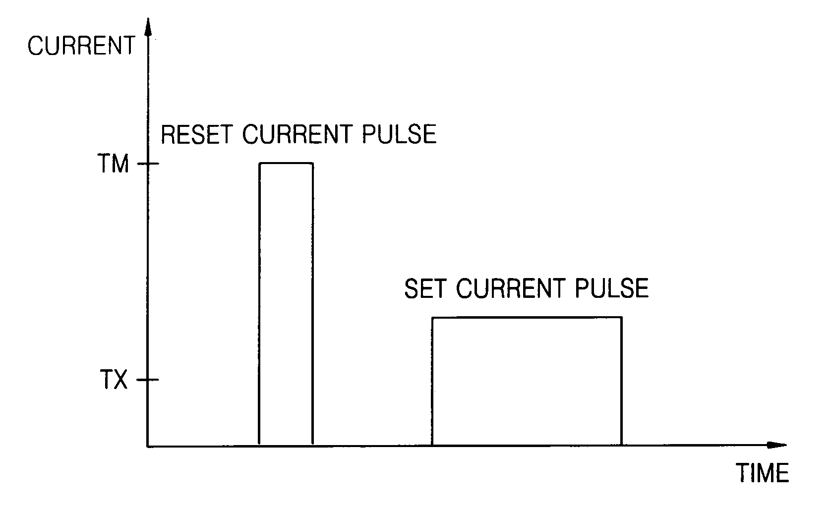
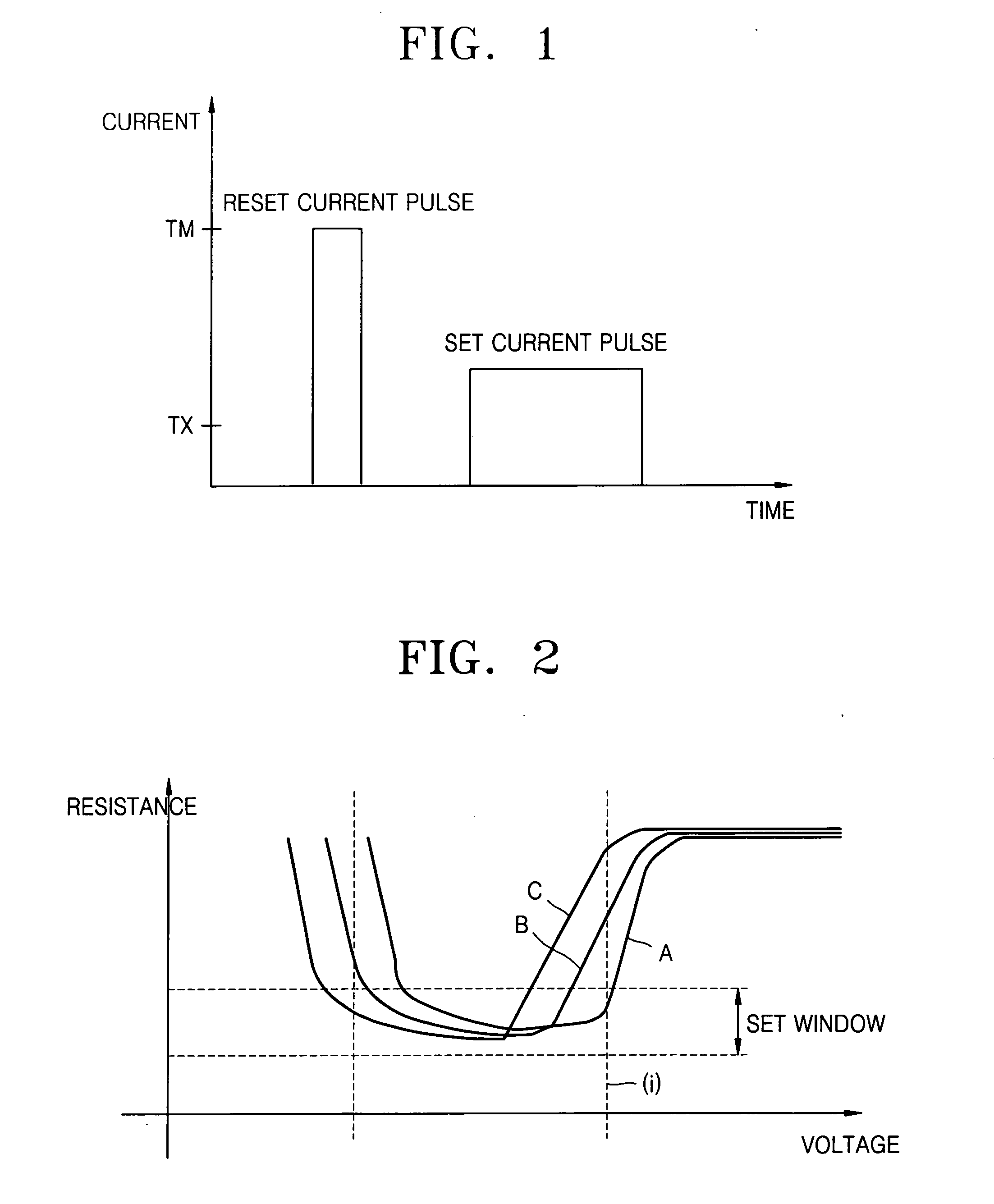
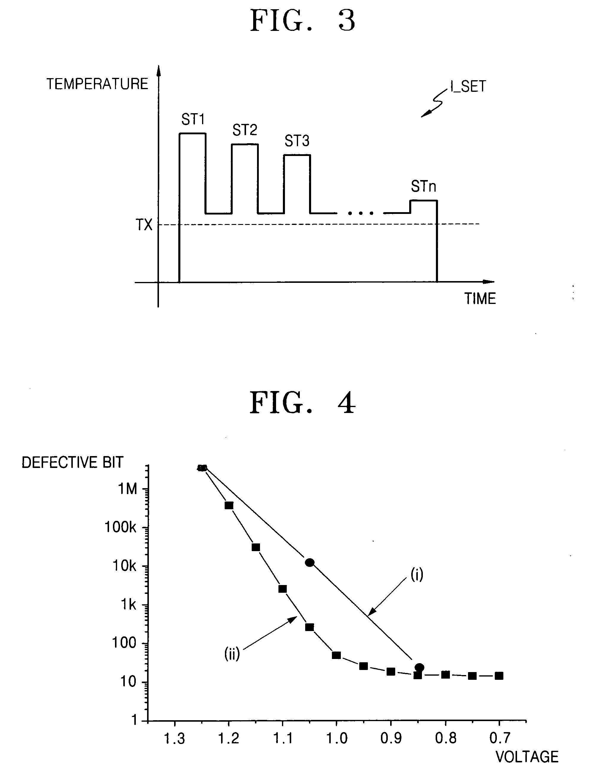
[0026]FIG. 3 is a graph illustrating a set current pulse applied to a phase-change memory array according to an exemplary embodiment of the present invention. In general, in order to program a phase-change memory array to a set state, a set current pulse may be applied to phase-change memory cells of the array. In an example, the set current pulse, I_SET, may include first through nth stages, ST1 through STn. In any given stage, the minimum current level may remain greater than a reference current value. The current level of the set current pulse I_SET may be reduced sequentially from stage to stage as it is applied to the phase-change memory cells of the array. The currents of the set current pulse l_SET may vary from memory cell to memory cell and / or among the memory cells of the phase-change memory array, but the current level of the set current pulse in the first stage ST1 is at the highest current that would cause a given phase-change cell in the memory array to transit to a se...


PUM


Abstract

A method for programming a phase-change memory array and circuit of a phase-change memory device, each having a plurality of phase-change memory cells, may enable all the phase-change memory cells therein to be changed or set at a set resistance state, and may reduce the time needed to change the phase-change memory array to the set resistance state. In the method, a set current pulse having first through nth stages may be applied to the cells of the array to change the cells to the set resistance state. A minimum current level of the set current pulse applied to the phase-change memory cells in any stage may be higher than a reference current level for the cells of the array. A given current level of the set current pulse may be sequentially reduced from stage to stage.

Description

CROSS-REFERENCE TO RELATED APPLICATIONS [0001] This application claims the priority of Korean Patent Application No. 2004-14954, filed on Mar. 5, 2004, in the Korean Intellectual Property Office, the disclosure of which is incorporated herein in its entirety by reference. BACKGROUND OF THE INVENTION [0002] 1. Field of the Invention [0003] The present invention relates, in general, to a method and circuit for programming a phase-change memory array to a set state. [0004] 2. Description of the Related Art [0005] Phase-change random access memories (PRAMs) are non-volatile memory devices that store data using a phase-change material, such as a chalcogenide (e.g., Ge—Sb—Te (GST)), the electric resistance of which varies upon a phase transition between two states that is caused by a change in temperature. PRAMs have many of the advantages of both volatile memories such as dynamic random access memories (DRAMs) and non-volatile memories, at a generally lower power consumption. [0006] If c...

Claims


Application Information

Patent Timeline
IPC IPC(8): G11C13/02G11C13/00G11C16/02G11C16/10G11C19/08H01L27/10H01L27/105H01L27/115
CPCG11C13/0004G11C13/0069G11C2013/0092G11C2013/0088G11C2013/0078
Inventor CHOI, BYUNG-GILKIM, DU-EUNGKWAK, CHOONG-KEUNCHO, BEAK-HYUNG
Owner SAMSUNG ELECTRONICS CO LTD
Why Eureka
Try Eureka