Method for fabricating vertical transistor
- Summary
- Abstract
- Description
- Claims
- Application Information
AI Technical Summary
Benefits of technology
Problems solved by technology
Method used
Image

Examples
Embodiment Construction
[0021] Reference will now be made in detail to exemplary embodiments of the present invention which are illustrated in the accompanying drawings. Wherever possible, the same reference numbers will be used throughout the drawings to refer to the same or like parts.
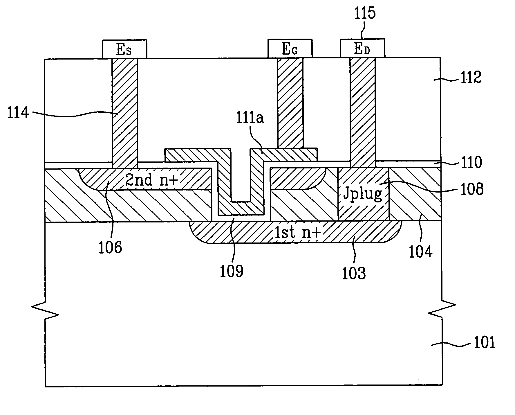
[0022] Hereinafter, a method for fabricating a vertical transistor according to the present invention will be described with reference to the accompanying drawings. FIG. 1A to FIG. 1F show cross sectional views of the fabrication process for a vertical transistor according to the present invention.
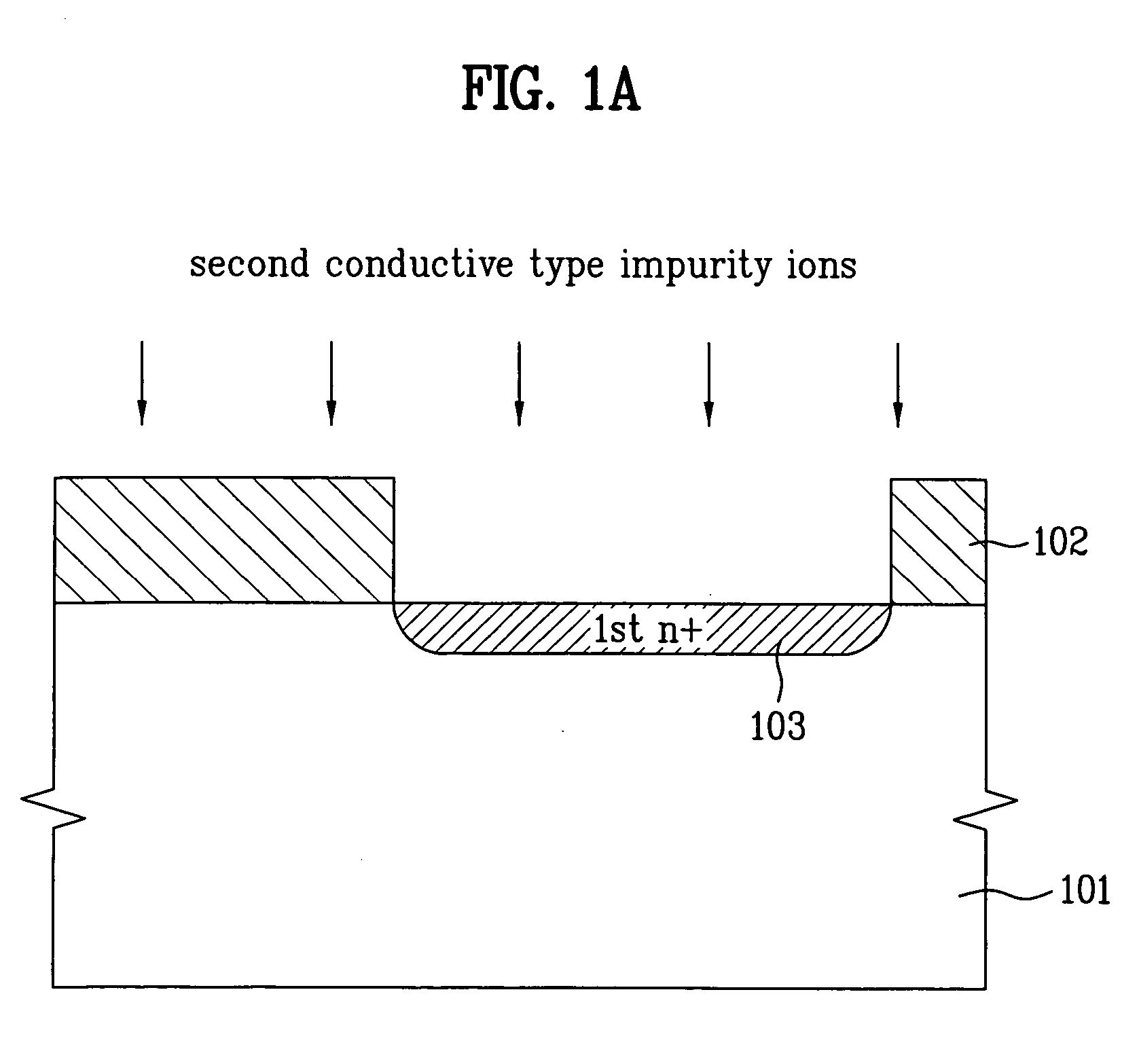
[0023] First, as shown in FIG. 1A, a semiconductor substrate 101 of mono-crystal silicon is prepared. The semiconductor substrate 101 may be formed of a first conductive type mono-crystal silicon, wherein the first conductive type may be n-type or p-type. For convenience of explanation, herein, the first conductive type will be referred to as the p-type.
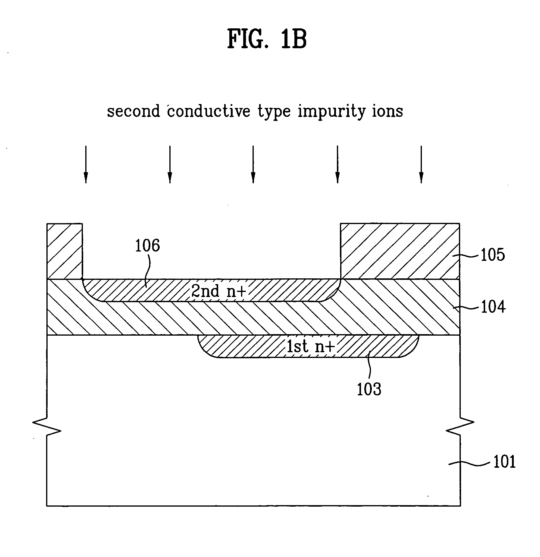
[0024] In this state, a photoresist layer is coated on an entire surface of...
PUM
 Abstract
Description
Claims
Application Information