Layered structure for electron device including regions of different wettability, electron device and electron device array that uses such a layered structure

a layer structure and electron device technology, applied in non-linear optics, instruments, optics, etc., can solve the problems of large patterning error that can reach as much as 10 m, offset printing is not considered suitable for formation of fine patterns, and the offset printing process suffers from large patterning error, so as to reduce the cost of the transistor provided by the electron device, the effect of reducing the use of resources and low cos

Inactive Publication Date: 2009-11-03
RICOH KK
View PDF33 Cites 25 Cited by
  • Summary
  • Abstract
  • Description
  • Claims
  • Application Information

AI Technical Summary

Benefits of technology

[0107]According to the sixteenth aspect of the present invention, it becomes possible to provide a high-performance electron device having a transistor structure with low cost with reduced use of resources. Particularly, it should be noted that the variable wettability layer functions as a gate insulation layer, and thus, the cost of the transistor provided by the electron device is reduced further.
[0108]According to the seventeenth aspect of the present invention, it becomes possible to minimize the gap or channel length between a pair of electrode layers constituting a source electrode and a drain electrode even when a low cost process of high efficiency of material use such as a printing process is used. Further, it becomes possible to increase the carrier mobility, and as a result, the performance of the transistor provided by the electron device is improved.
[0109]By employing an ink-jet process that supplies minute droplets of the liquid in the method of fabricating an electron device of the seventeenth aspect as set forth in the eighteenth aspect of the present invention, the effect of surface energy of the variable wettability layer increases, and thus, the present invention is advantageous for the fabrication of the layered structure that utilizes the feature of the variable wettability layer.
[0110]By using ultraviolet radiation in the method of fabricating an electron device of the seventeenth or eighteenth aspect as set forth in the nineteenth aspect of the present invention, it becomes possible to provide a fabrication method of an electron device capable of forming the gap (channel length) between a pair of electrode layers constituting a source electrode and a drain electrode by a process conducted in an atmospheric ambient without causing damages in the interior of the layered structure.
[0111]According to the twentieth aspect of the present invention, there is provided an array of electron devices in which the electron device of the fourteenth through sixteenth aspect is provided on a substrate with plural numbers, and thus, it becomes possible to provide a high-performance electron device array with low cost and with reduced use of resources.
[0112]According to the twenty-first aspect of the present invention, the display device uses the electron device array of the twentieth aspect, and thus, it becomes possible to provide a display device of high image quality at low cost with reduced use of resources.

Problems solved by technology

On the other hand, the offset printing process as disclosed in Patent Reference 1 suffers from the problem of large patterning error that can reach as much as ±10 μm when the patterning size error and positioning error are added.
Thus, offset printing is not deemed suitable for formation of fine patterns.
In the case of the process that uses ink-jet printing as set forth in Non-patent Reference 1, there arises a problem that the maximum resolution achievable by such a process is only 30 μm when an ordinary ink-jet head designed for common printers is used.

Method used


Image

  • Layered structure for electron device including regions of different wettability, electron device and electron device array that uses such a layered structure
  • Layered structure for electron device including regions of different wettability, electron device and electron device array that uses such a layered structure
  • Layered structure for electron device including regions of different wettability, electron device and electron device array that uses such a layered structure

Examples


example 1

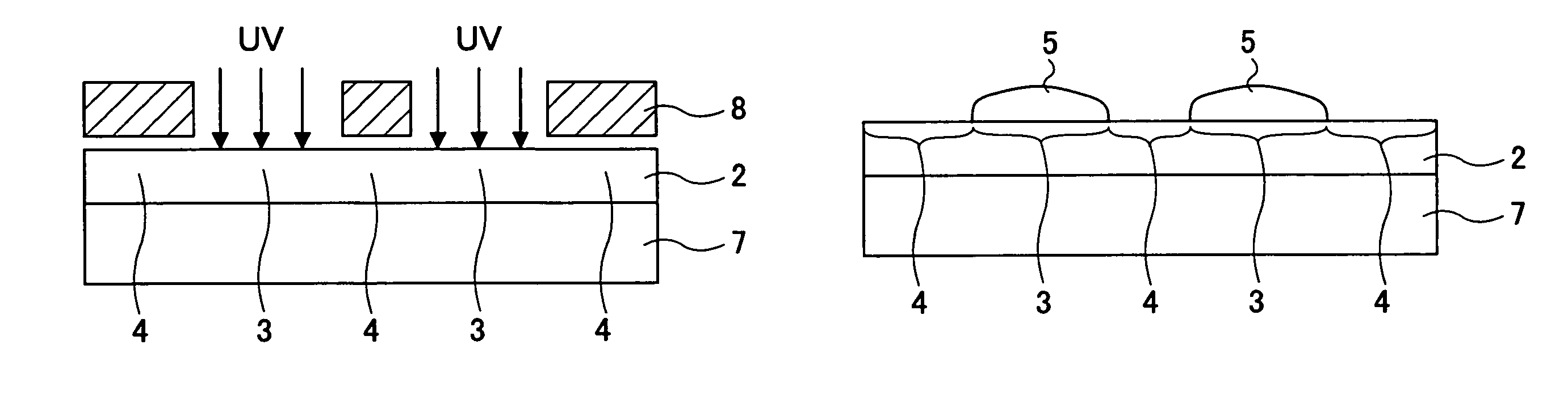
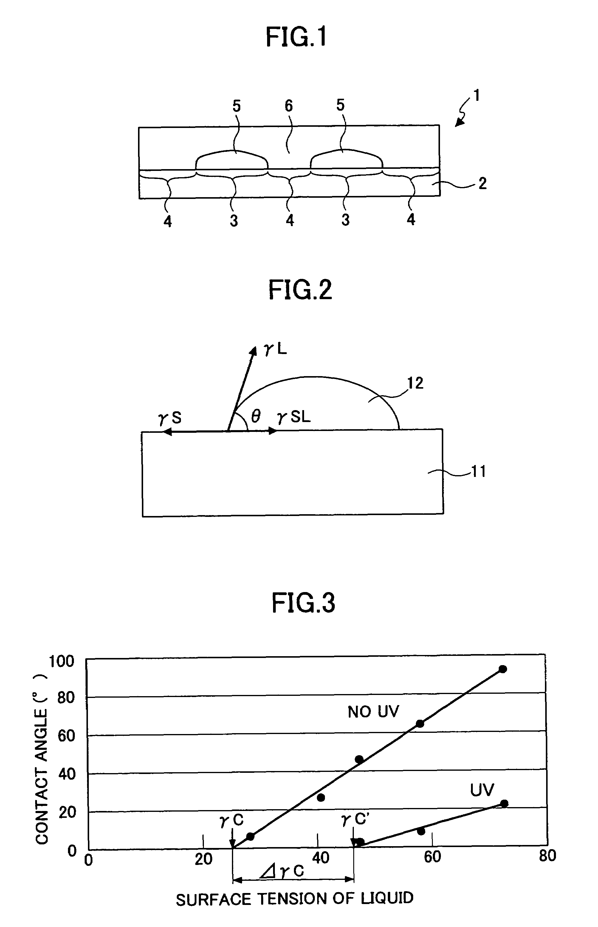
[0247]Example 1 relates to fabrication of an electron device having a structure similar to that of the electron device (TFT) 31 shown in FIG. 7.

[0248]First, a mixed solution dissolving therein the precursor of the materials having the structure shown in chemical formula 6 and chemical formula 7 after baking is applied on the glass substrate 7 by a spin coating process as the variable wettability layer 2. Thereafter, baking is conducted at 280′.

[0249]

[0250]In order to evaluate the characteristics of the variable wettability layer 2, following experiments were conducted separately.

[0251](1) By using an UV lamp for an optical source, the distance between the optical source and the substrate is adjusted such that there is realized an optical intensity of 5 mW / cm2 at the wavelength of 250 nm on the substrate. Next, the radiation doze is changed by changing the duration of irradiation for the wavelength of 250 nm and the change of contact angle of the layer 2 to water is observed.

[0252]FI...

example 2

[0267]In Example 2, the precursors that form the structures of chemical formulae 8-11 below after baking are applied on the glass substrate under the same condition as Example 1 in the form of a solution mixed with the precursor of the structure represented by chemical formula 7 noted before.

[0268]

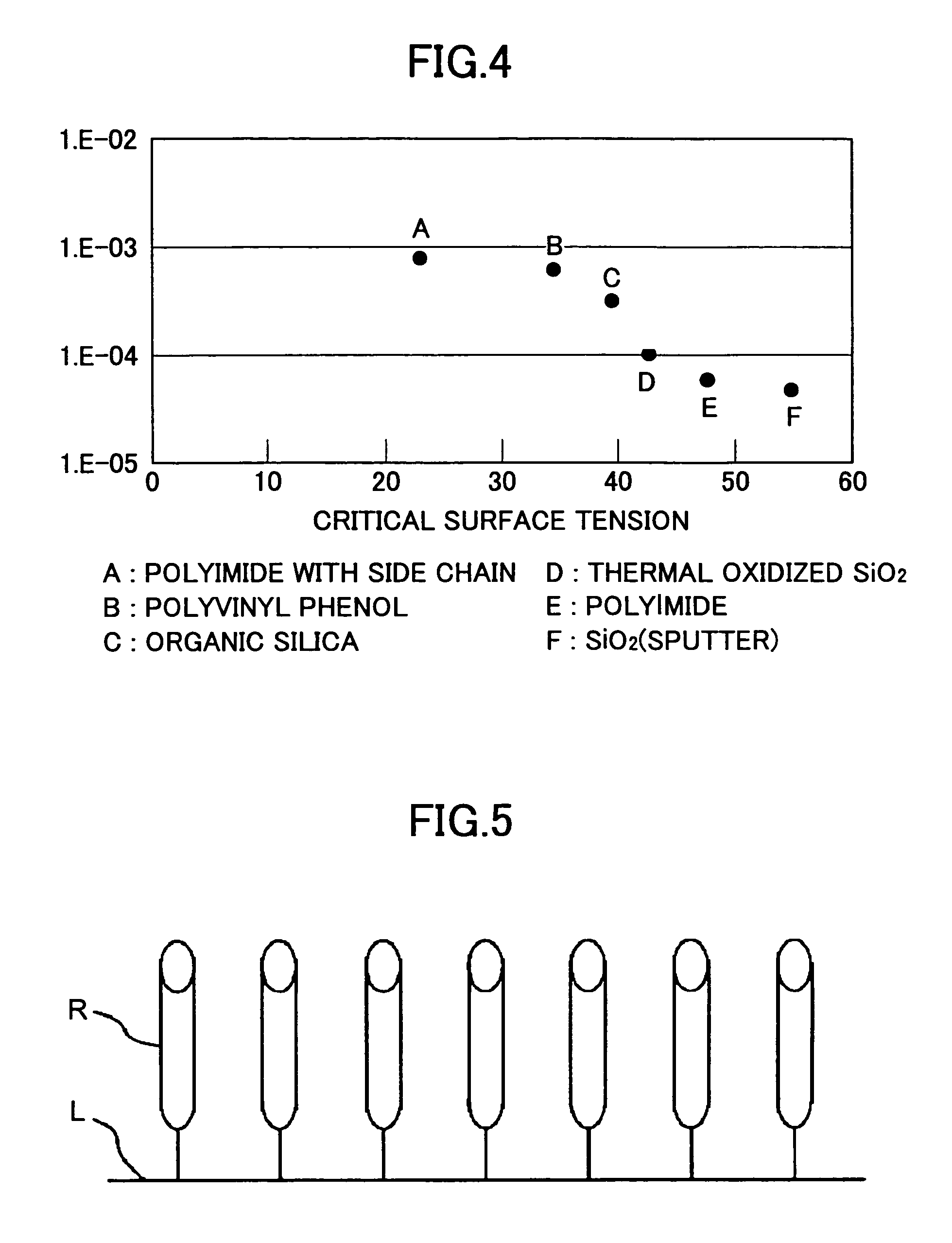
[0269]Next, the contact angle is measured for several liquids of different surface energies before and after irradiation of ultraviolet radiation with the dose of 9 J / cm2, and the critical surface tension is obtained similarly to the case of Example 1.

[0270]The results thereof are summarized in Table 2 below.

[0271]

TABLE 2FormulaFormulaFormulaFormula891011Before UV18 mN / m21 mN / m26 mN / m28 mN / mirradiationAfter UV44 mN / m43 mN / m41 mN / m42 mN / mirradiation

[0272]From Table 2, it can be seen that the critical surface tension takes the value of 18-28 mN / m in the case no ultraviolet irradiation is made while the critical surface tension takes the value of 41-44 mN / m after the ultraviolet irradiation i...

example 3

[0273]In Example 3, the mixed solution used in Example 2 is applied on a glass substrate under the same film forming condition as Example 4. Next, patterning is conducted under the condition similar to that of Example 4 and the source and drain electrodes are formed by an ink-jet process. After this, the semiconductor layer is formed by a spin coating process while using a polymer 1 represented by chemical formula 12 for the organic semiconductor material.

[0274]Table 3 below shows comparison of the mobility and On / Off ratio for the TFT thus fabricated to have the structure shown in FIG. 8.

[0275]

TABLE 3FormulaFormulaFormulaFormula891011Mobility4 × 10−32 × 10−36 × 10−44 × 10−4(cm2 / Vs)On / Off28201260860485ratio

[0276]Thus, a result similar to the case of Example 4 below that uses the same organic semiconductor is obtained also in the case of using any of the polyimide materials such as the polyimide represented by the chemical formulae 8 and 9 in which the constituting unit of the princi...


PUM

PropertyMeasurementUnit
critical surface tensionaaaaaaaaaa
widthaaaaaaaaaa

Abstract

A layered structure comprises a variable wettability layer including a material that changes a critical surface tension in response to energy provided thereto, the wettability changing layer including at least a high surface energy part of large critical surface tension and a low surface energy part of low critical surface tension, a conductive layer formed on the variable wettability layer at the high surface energy tension part, and a semiconductor layer formed on the variable wettability layer at the low surface energy part.

Description

CROSS-REFERENCE TO RELATED APPLICATIONS[0001]The present invention is based on Japanese priority applications 2003-156314 filed on Jun. 2, 2003, 2004-86388 filed on Mar. 24, 2004, and 2004-124292 filed on Apr. 20, 2004, the entire contents of which are incorporated herein as reference.BACKGROUND OF THE INVENTION[0002]The present invention relates to layered structures suitable for thin-film transistors (TFT), and the like, electron devices such as TFT that uses such a layered structure, fabrication method thereof, electron device arrays and display apparatuses.[0003]A flat panel display apparatus such as a liquid crystal display (LCD) panel, plasma display panel (PDP), organic electro-luminescence (EL) device, and the like, generally includes a part formed by patterning a thin film layer, as in the case of active devices such as an MIM (metal-insulator-metal) device or TFT or a light-emitting device.[0004]Meanwhile, a device that uses an organic material for a part thereof or for th...

Claims


Application Information

Patent Timeline
Patent Type & Authority Patents(United States)
IPC IPC(8): H01L23/48H01L23/52H01L29/40G02F1/1368H01L21/28H01L21/288H01L21/336H01L29/786H01L51/05H01L51/40
CPCH01L51/0004H01L51/0022H01L29/6675H01L2924/0002H01L2924/00H10K71/13H10K71/611
Inventor TANO, TAKANORIFUJIMURA, KOHTOMONO, HIDENORIKONDOH, HITOSHI
Owner RICOH KK
Why Eureka
Try Eureka