Compound for forming wiring conductor, fabrication method of circuit board using the same and circuit board

a technology of wiring conductors and compounded circuit boards, which is applied in the direction of conductive pattern formation, capacitors, and conductive patterns, can solve the problems of inability to obtain ink discharge ports, and inability to obtain desired patterns, etc., to achieve the effect of reducing resistivity, improving strength as a conductor, and forming sure and inexpensively

Inactive Publication Date: 2005-09-22
HITACHI CABLE
View PDF8 Cites 49 Cited by
  • Summary
  • Abstract
  • Description
  • Claims
  • Application Information

AI Technical Summary

Benefits of technology

[0041] Specifically, it is the first object of the present invention to provide a conductor paste which comprises a new composition and can be sintered at low temperature and which can solve the first problem (low conductor occupying ratio) in the third conventional technology.
[0062] (5) By providing electrochemical treatment such as plating, etc. after sintering, the void formed by removal of dispersed medium during sintering is filled with the conductor, so that the electrical resistance formed at the wiring conductor portion can be reduced as compared to the case with no filling treatment provided for the void as well as strength can be improved.

Problems solved by technology

When fine wiring is formed by the use of the second conventional technology, low-viscosity ink is used to discharge (eject) superfine ink drops accurately by ink-jet printing, and as a result, there is a problem of ink bleed and instability of ink shape when resist patterns of film thickness that can stand the plating process or etching process are formed.
However, because the conductor surface roughness greatly affects adhesion of resist, restricting to the surface roughness range cannot secure resist adhesion, and generates exfoliation or crack of resist in the process of being plating or etching, and as a result, it is likely to cause such a problem that the desired patterns are unable to be obtained.
In addition, because superfine accurate shaping of ink discharge port (i.e. ink jet nozzle) is essential to accurately discharge superfine ink droplets by ink jet printing, it is difficult to obtain the ink discharge port.
Furthermore, in order to efficiently form resist film in a wide area by superfine ink droplets, it is desirable to arrange a large number of highly accurate ink discharge ports in a line, but the inkjet printer that has such a large number of juxtaposed highly accurate ink discharge ports inevitably costs high, and the printer can not solve the problem of the first conventional technology concerning the apparatus price.
Conversely, a great deal of troublesome work is required to maintain the highly accurate ink discharge ports, possibly creating a new problem.
On the other hand, in the third conventional technology, resist is not inherently used and no adhesion problem between the substrate and resist occurs, but a new problem arises from printing liquid paste containing superfine particles.

Method used


Image

  • Compound for forming wiring conductor, fabrication method of circuit board using the same and circuit board
  • Compound for forming wiring conductor, fabrication method of circuit board using the same and circuit board
  • Compound for forming wiring conductor, fabrication method of circuit board using the same and circuit board

Examples


embodiment 1

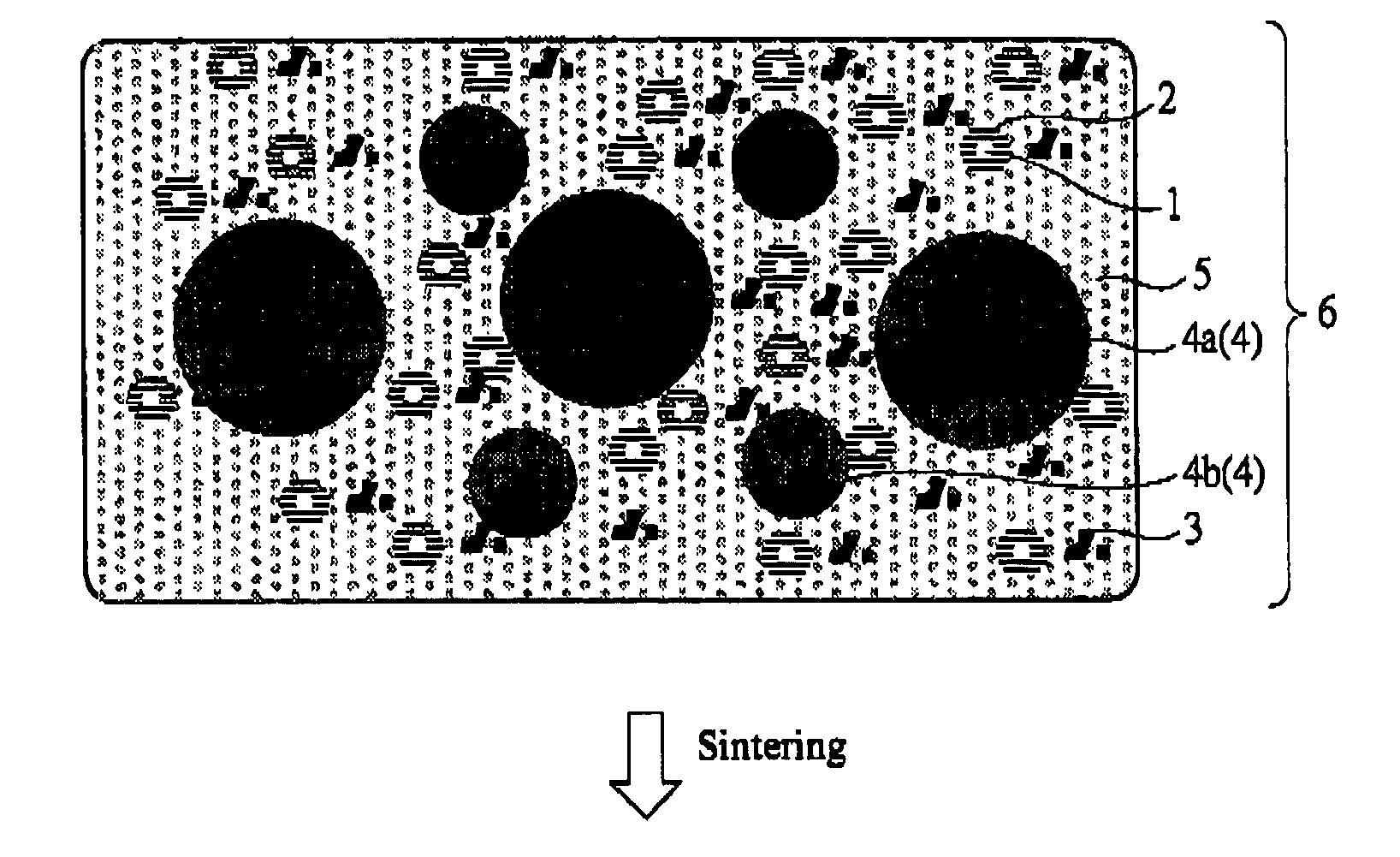
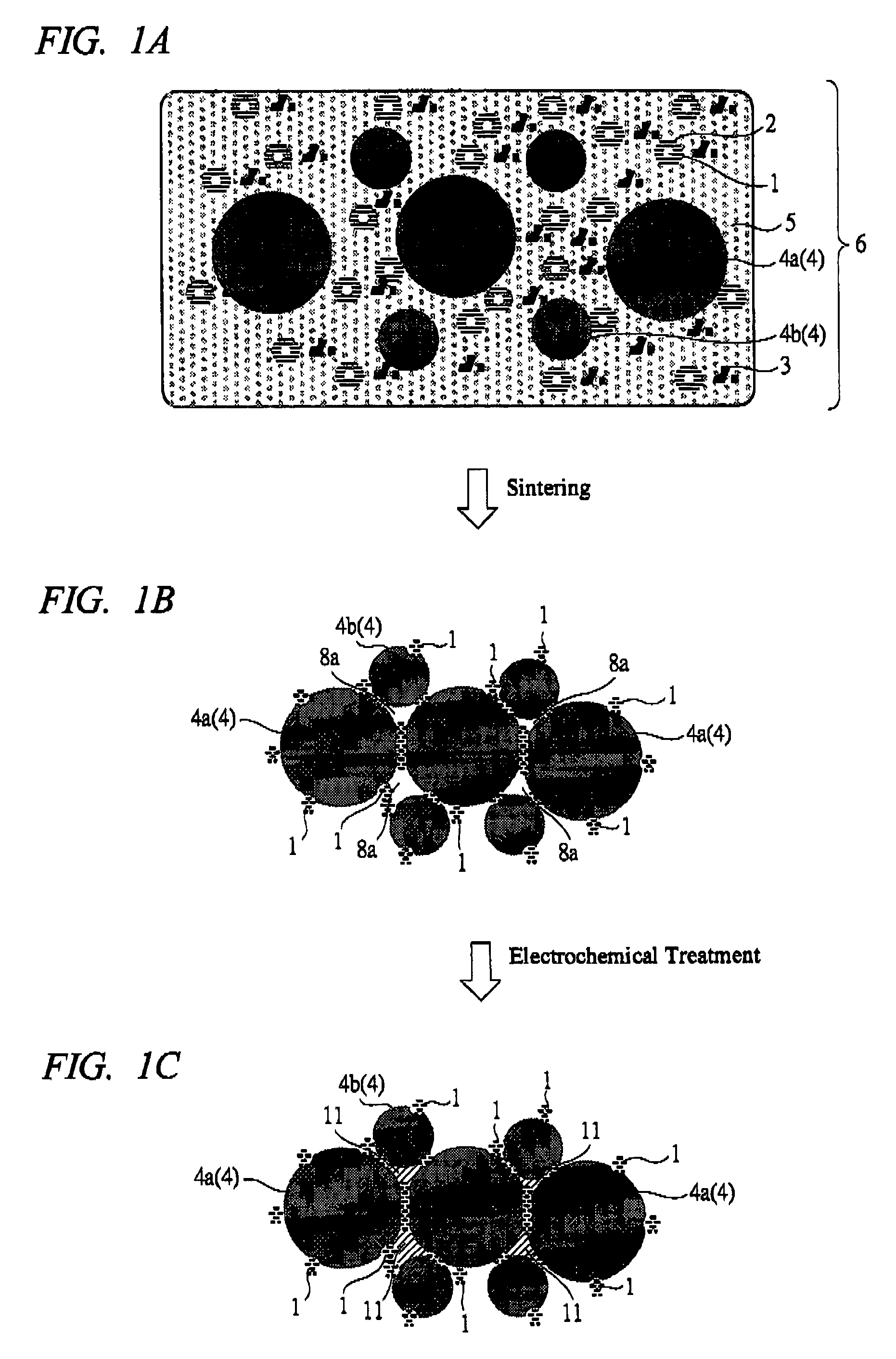
[0068] First of all, in embodiment 1, a compound (and a composition thereof) for forming wiring conductor, one of the technologies proposed by the present invention, will be described.

[0069] As shown in FIG. 1A, compound for forming wiring conductor 6 related to the present invention contains: [0070] (a) superfine metal particles (metal nanoparticles) 1 whose average particle size is 1 through 10 nm; [0071] (b) an organic coating compound 2 coated on the surface of the superfine metal particle 1 in the film thickness of 1 through 10 nm; [0072] (c) a latent reactive organic compound 3 that reacts with the organic coating compound in the range from 100 to 250° C.; [0073] (d) metal particles 4 whose average particle size is 0.5 through 10 μm; and [0074] (e) dispersion medium 5 that stably disperses components (a) through (d).

[0075] The superfine metal particles 1 suited for the present invention are so-called metal nanoparticles of average particle size between 1 and 10 nm. For this ...

embodiment 2

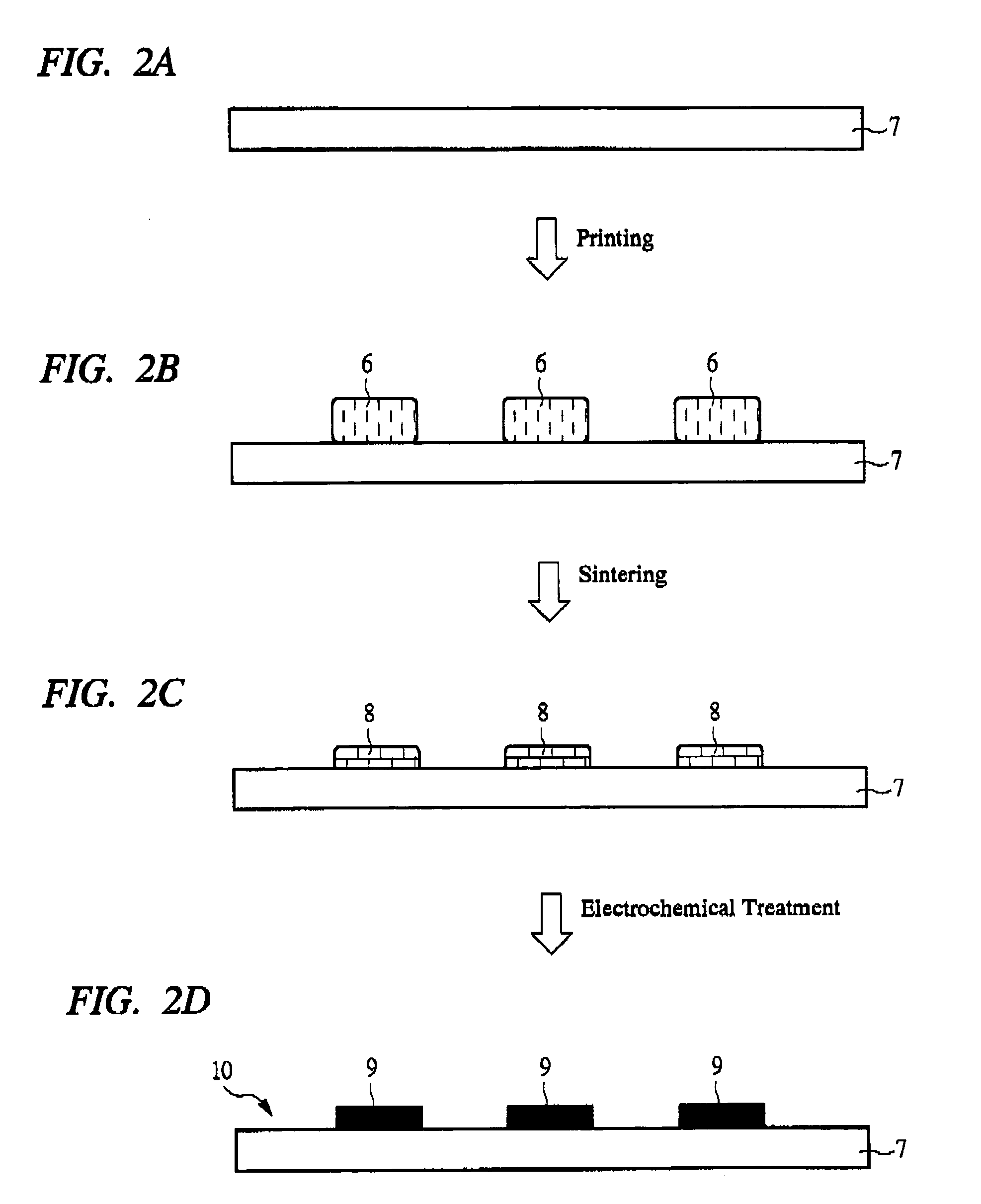
[0106] In the embodiment 2, a circuit board for which the wiring conductor fabricated by the use of the compound for forming wiring conductor related to the present invention described in the embodiment 1 is used and the wiring conductor is at least partially used and fabrication method thereof will be described.

[0107] By using the compound for forming wiring conductor 6 proposed by the present invention, the wiring conductor can be conveniently formed, and by using this wiring conductor at least for part of it, a circuit board can be fabricated at low cost and in a short time.

[0108]FIG. 2A shows a substrate 7 that serves as a base of the circuit board. As shown in FIG. 2B, on the surface of the substrate 7, the compound for forming wiring conductor 6 is formed into film to have a desired pattern shape. Thereafter, as shown in FIG. 2C, by heating treatment the substrate in such a manner that the pattern portion is sintered, a wiring conductor 8 with the desired pattern can be obta...


PUM

PropertyMeasurementUnit
particle sizeaaaaaaaaaa
thicknessaaaaaaaaaa
particle sizeaaaaaaaaaa

Abstract

The present invention sufficiently secures conductor component content ratio in wiring formed on a multilayer circuit board and increases reliability by fabricating the multilayer circuit board by steps of drawing wiring precursor patterns containing a paste of compound for forming wiring conductor containing (a) superfine metal particles (metal nanoparticles) whose average particle size is 1-10 nm; (b) an organic coating compound coated on the surface of the superfine metal particle in the film thickness of 1-10 nm; (c) a latent reactive organic compound reacting with the organic coating compound in the range of 100-250° C., (d) metal particles whose average particle size is 0.5-10 μm, and (e) dispersion medium that stably disperses components (a) through (d) on a substrate by screen printing, sintering by heating the patterns to 100-250° C., and electrochemically treating the patterns to allow the conductor to deposit in a desired cross-sectional area in the inside.

Description

CROSS-REFERENCE TO RELATED APPLICATION [0001] The present application claims priority from Japanese Patent Application No. JP 2003-415557 filed on Dec. 12, 2003, the content of which is hereby incorporated by reference into this application. TECHNICAL FIELD OF THE INVENTION [0002] The present invention relates to a printed circuit board technology and more specifically, to a conducting compound for forming a circuit board at low cost and in a short time, a fabrication method of a circuit board with conductor patterns that can be formed at low cost and in a short time using the relevant conducting compound, and to the circuit board. BACKGROUND OF THE INVENTION [0003] As a multilayer circuit board fabrication method, a large variety of methods have been designed, and the methods can be classified from several points of view and used properly in accord with their characteristics. [0004] For example, to classify the printed circuit board fabricating methods with focusing on the conducto...

Claims


Application Information

Patent Timeline
Patent Type & Authority Applications(United States)
IPC IPC(8): B22F1/052B22F1/0545B22F1/102B22F7/04H01B1/00H01B1/22H05K1/09H05K3/12H05K3/24
CPCB22F1/0014B22F1/0022B22F1/0062B22F2998/00B82Y30/00Y10T428/24917H05K3/245H05K1/097B22F1/0545B22F1/052B22F1/102
Inventor YAMAGUCHI, YOSHIHIDE
Owner HITACHI CABLE
Why Eureka
Try Eureka