Micromirror element and optical switch
- Summary
- Abstract
- Description
- Claims
- Application Information
AI Technical Summary
Benefits of technology
Problems solved by technology
Method used
Image

Examples
first embodiment
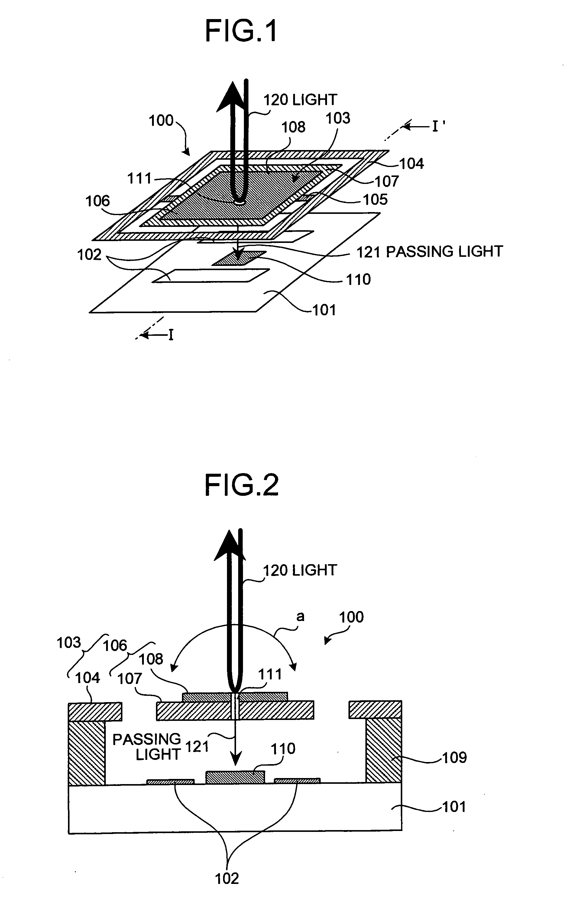
[0040]FIG. 1 is a perspective view of a micromirror element 100 according to the present invention. FIG. 2 is a cross section along a I-I′ line in FIG. 1.
[0041] The micromirror element 100 has a structure in which a mirror body 103 is supported by a support 109 (see FIG. 2) on a wiring substrate 101 where a pair of mirror drive electrodes 102 and a light detection device 110 are arranged. Although not specifically shown, various wiring and circuits are arranged on the wiring substrate 101.
[0042] As shown in FIG. 1, the mirror body 103 comprises a mirror frame 104 that is a square frame body and a square movable mirror 106. The movable mirror 106 is swayably supported by the mirror frame 104 via a pair of torsion bars 105 arranged opposite to each other on the edge sides of the movable mirror 106. The mirror frame 104 is mounted and fixed to the edge portion of the support 109 (see FIG. 2).
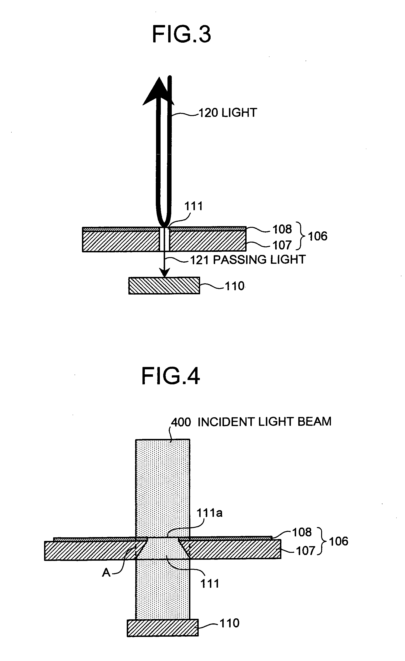
[0043] The movable mirror 106 has a reflecting layer 108, i.e., a reflecting surface, formed ...
sixth embodiment
[0091]FIG. 12 is a cross sectional view of a micromirror element according to the present invention.
[0092] As shown in FIG. 12, the light detection device 110 is mounted on the wiring substrate 101 in the micromirror element 100 of the present embodiment. The mirror body 103 is arranged on the wiring substrate 101 via bumps for connection 1201.
[0093] The mirror body 103 is constituted of the mirror frame 104 supported by the bumps for connection 1201 and the movable mirror 106 supported by the mirror frame 104 that is supported swayably by the torsion bars (not shown), similarly to the case of the first embodiment. Although the movable mirror 106 has the same configuration as that of the first embodiment, an electrode for mirror side is not formed on the back surface of the mirror substrate 107, which is different from the first embodiment.
[0094] According to the present embodiment, a pair of comb electrodes 1202A are arranged on the inner periphery of the mirror frame 104 so as t...
seventh embodiment
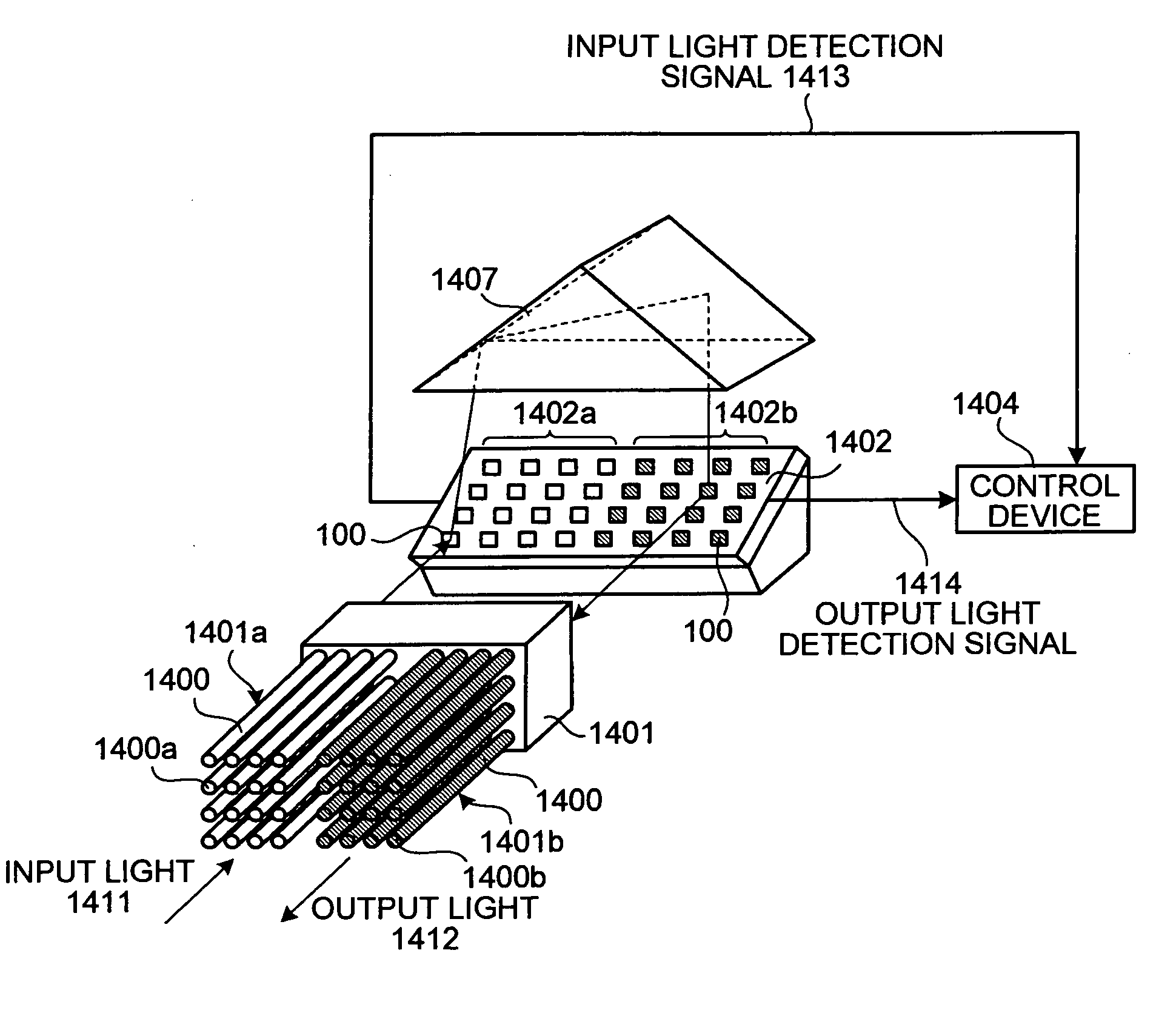
[0099]FIG. 13 is a block diagram of an optical switch according to the present invention.
[0100] As shown in FIG. 13, the optical switch of the present embodiment is provided with a fiber array for input side 1301 constituted of a plurality of optical fibers 1300A arranged with each one end of the optical fibers 1300A constituting optical input ports 1300B, a mirror array for input side 1303 and a mirror array for output side 1304 both with a plurality of the micormirror elements 100 of the above structure arranged and integrated in a matrix form, a fiber array for output side 1302 constituted of a plurality of optical fibers 1300A arranged with each one end of the optical fibers 1300A constituting optical output ports 1300C, and a control device 1305 to which detection signals of the light detected by each light detection device 110 of each micromirror element 100 constituting the mirror array for input side 1303 and the mirror array for output side 1304 are transmitted to carry out...
PUM
 Abstract
Description
Claims
Application Information
 - Generate Ideas
- Intellectual Property
- Life Sciences
- Materials
- Tech Scout
- Unparalleled Data Quality
- Higher Quality Content
- 60% Fewer Hallucinations
Browse by: Latest US Patents, China's latest patents, Technical Efficacy Thesaurus, Application Domain, Technology Topic, Popular Technical Reports.
© 2025 PatSnap. All rights reserved.Legal|Privacy policy|Modern Slavery Act Transparency Statement|Sitemap|About US| Contact US: help@patsnap.com