Photosensitive resin composition, resist pattern forming method, substrate processing method, and device manufacturing method

Inactive Publication Date: 2005-10-06
CANON KK
View PDF11 Cites 19 Cited by
  • Summary
  • Abstract
  • Description
  • Claims
  • Application Information

AI Technical Summary

Benefits of technology

[0024] According to the present invention, it is possible to realize a photosensitive resin composition which can form a high-resolution resist pattern with a low line edge roughness and can be used i

Problems solved by technology

In these circumstances, it has become difficult to accurately form a thick resist pattern with a high aspect ratio.
In the above described two-layer resist process, as an upper layer resist, a silicon-containing resist is required but is accompanied with such a problem that the silicon-containing resist has a low resolution to provide a large li

Method used


Image

  • Photosensitive resin composition, resist pattern forming method, substrate processing method, and device manufacturing method
  • Photosensitive resin composition, resist pattern forming method, substrate processing method, and device manufacturing method
  • Photosensitive resin composition, resist pattern forming method, substrate processing method, and device manufacturing method

Examples


Example

[0027] A first embodiment of a photosensitive resin composition according to the first aspect of the present invention will be explained.

[0028] The photosensitive resin composition contains the components (A) and (B) described above and is capable of providing a high resolution (resolving power) and a high aspect ratio.

[0029] By using a photosensitive resin composition (hereinafter, simply referred to as a “resist”), it becomes possible to form a resist pattern which is low (small) in line edge roughness (“LER”) and high in aspect ratio through a surface imaging with arbitrary exposure method and subsequent selective sylylation process and dry development.

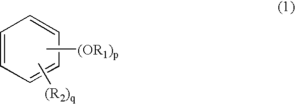
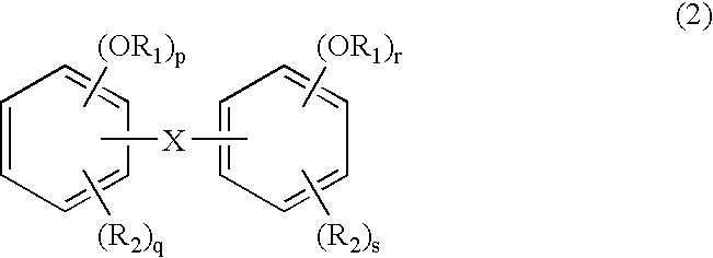
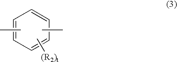
[0030] In this embodiment, as the polymer for the component (A), e.g., it is possible to use acrylic-based resin, styrene-based resin, epoxy-based resin, amide-based resin, amide-epoxy-based resin, alkyd-based resin, phenol-based resin, and the like. Of these resins, it is preferable that they does not contain hydroxyl group, ca...

Example

[0055] Next, a second embodiment of a photosensitive resin composition according to the second aspect of the present invention will be described.

[0056] The photosensitive resin composition in this embodiment is characterized by containing a polymer, as a component (A), having a monodisperse molecular weight; a radiation-sensitive acid generation agent as a component (C); and a compound, as a component (D), containing at least one functional group selected from the group consisting of hydroxyl group, carboxyl group, amino group, thiol group, and amido group, each of which is protected by an acid-dissociative group.

[0057] In this embodiment, the component (A) is the same as in the first embodiment described above.

[0058] The radiation-sensitive acid generation agent (hereinafter referred to as a “photoacid generator”) is a compound which includes chemical reaction by irradiation of radiation such as infrared radiation, visible radiation, ultraviolet radiation, 4t for ultraviolet rad...

Example

(Embodiments 1-4 and Comparative Embodiments 1 and 2)

[0086] In these embodiments, photosensitive resin compositions associated with the above described photosensitive resin composition according to the first aspect of the present invention are prepared in formulations shown in Table 1 below. TABLE 1Amount (g)Comp.Comp.ComponentMaterialEmb. 1Emb. 2Emb. 3Emb. 4Emb. 1Emb. 2(A)polystyrene*1300000(A)polystyrene*2030000(A)polystyrene*3001000(A)polystyrene*4000030(A)polystyrene*5000003(B)TM-3007791077solventPGMEA909090909090

*1Mw = 5200, Mw / Mn = 1.06

*2Mw = 2200, Mw / Mn = 1.06

*3Mw = 20000, Mw / Mn = 1.06

*4Mw = 5800, Mw / Mn = 2.0

*5Mw = 6500, Mw / Mn = 2.5

[0087] Each of the above prepared resist solutions is applied onto a silicon substrate and pre-baked on a hot plate at 100° C. for 60 sec., to form a resist layer having a thickness of 1.0 micron.

[0088] The substrate is imagewise exposed to light by i-ray stepper (wavelength=365 nm) as an exposure apparatus.

[0089] The exposed substrate is ...


PUM


Abstract

A photosensitive resin composition is constituted by a polymer, as a component (A), having a monodisperse molecular weight distribution; and a compound, as a component (B), first generating a functional group which is capable of being silylated by radiation irradiation.

Description

FIELD OF THE INVENTION AND RELATED ART [0001] The present invention relates to a photosensitive resin composition, a method of forming a resist pattern, a method of processing a substrate, and a device manufacturing method. Particularly, the present invention relates to a photosensitive resin composition (resist) and a method of forming a resist pattern using the resist. [0002] In recent years, demands for high density and high integration of devices have been increasing more and more in the fields of various electronic devices, requiring microprocessing, represented by a semiconductor device. In order to satisfy the demands, fine pattern formation has become essential. In a production process of such a semiconductor device, photolithography plays an important role in forming a fine pattern. [0003] In a photolithographic step, a single-layer resist has been conventionally used. However, the use of the single-layer resist is liable to increase a difference in level or an inclination ...

Claims


Application Information

Patent Timeline
IPC IPC(8): G03C1/492G03F7/023G03F7/039G03F7/38
CPCG03F7/0233G03F7/0392G03F7/38
Inventor ITO, TOSHIKIYAMAGUCHI, TAKAKO
Owner CANON KK
Why Eureka
Try Eureka