Method for manufacturing a master of an optical information recording medium, method for forming a pattern, a master, a stamper, an optical information recording medium and a resist

a technology of optical information and recording medium, which is applied in the field of manufacturing masters of optical information recording medium, masters, stampers, optical information recording mediums and resists, can solve the problems of difficult manufacture of resists, light sources, optical components, and no document clearly describing a specific resist and a method, and achieves a wide wavelength range, high environmental resistance, and high ratio of remaining films

Inactive Publication Date: 2005-03-03
PANASONIC CORP
View PDF7 Cites 3 Cited by
  • Summary
  • Abstract
  • Description
  • Claims
  • Application Information

AI Technical Summary

Benefits of technology

[0022] According to the present invention, a method of manufacturing a master of an optical information recording medium, a method for forming a pattern, a master itself, a stamper, an optical information recording medium and a resist can be obtained, which: enable heat-mode recording; enable use of conventional development equipment; and have a resist with high environmental resistance, which can absorb a wide wavelength range, has a high ratio of remaining film upon development, and has low line edge roughness.

Problems solved by technology

Furthermore, an electron beam may also be used for exposure, and use and manufacture of a resist, a light source, and optical components is becoming more difficult.
However, there is no document that clearly describes a specific resist and a method for forming a pattern using a chalcogen compound.
As a result, it was found that the material has very low contrast with respect to development, meaning there are substantial practical problems such as the ratio of remaining film and the line edge roughness.

Method used


Image

  • Method for manufacturing a master of an optical information recording medium, method for forming a pattern, a master, a stamper, an optical information recording medium and a resist
  • Method for manufacturing a master of an optical information recording medium, method for forming a pattern, a master, a stamper, an optical information recording medium and a resist
  • Method for manufacturing a master of an optical information recording medium, method for forming a pattern, a master, a stamper, an optical information recording medium and a resist

Examples


embodiment 1

[0037] (Embodiment 1)

[0038] The resist of the present invention works as a positive type resist by means of the alkali development process. A mechanism thereof will be described, and details of its composition will be described with reference to experimental results. The material TeOx is well known as a phase change material and is commercialized in a write-once, read-many type optical disk, for example. The present inventors discovered the phenomenon that alkali solubility of TeOx is increased by crystallization due to exposure and a mechanism thereof. The present inventors also found that the alkali solubility of unexposed portions (uncrystallized portions) is lowered when a stabilizing additive is added that is a material having a lower solubility than TeO2 in an alkaline environment, and that the ratio of remaining film and the line edge roughness are improved. This mechanism is thought to be as follows.

[0039] The material TeOx in the resist of the present invention is in an am...

embodiment 2

[0056] (Embodiment 2)

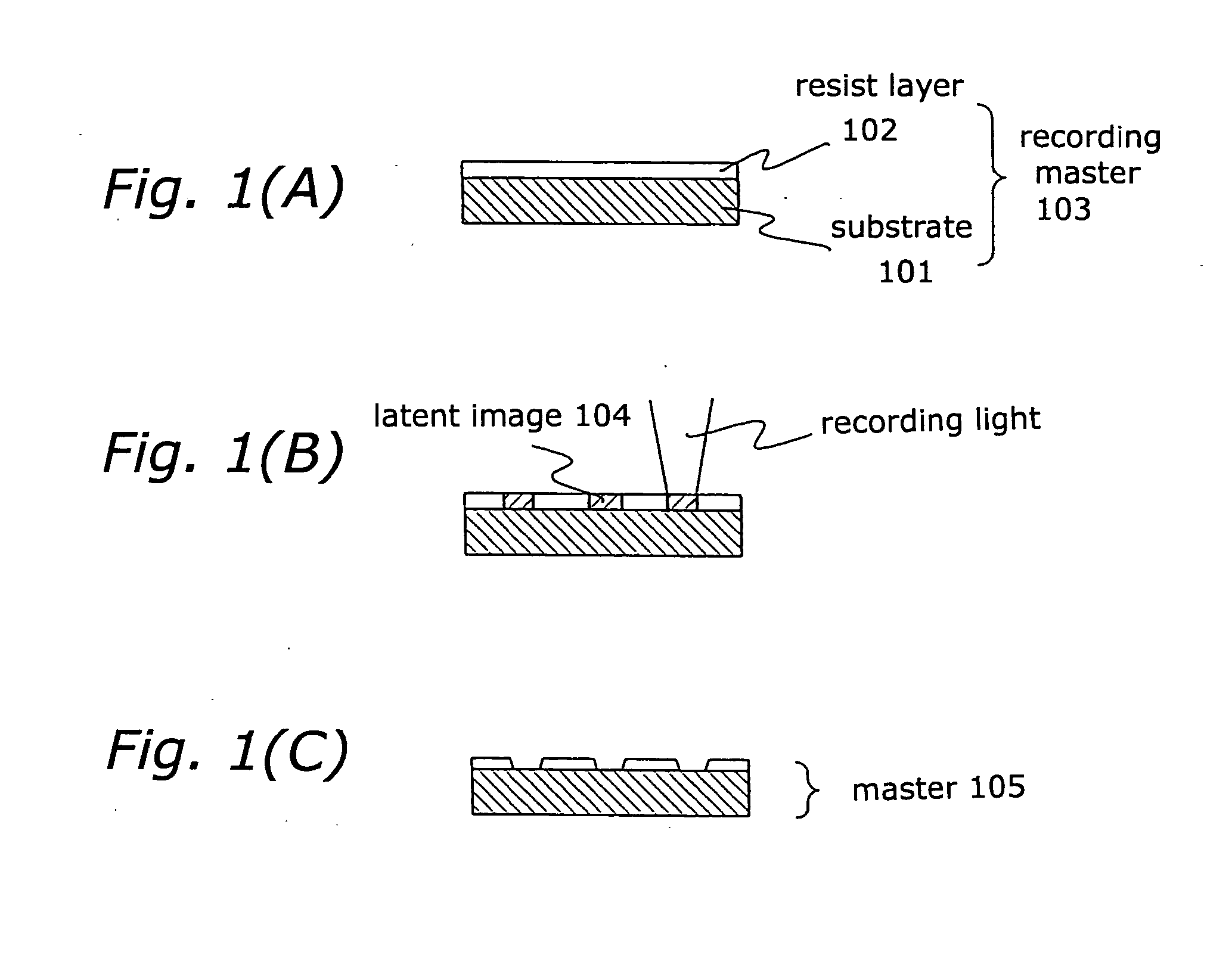
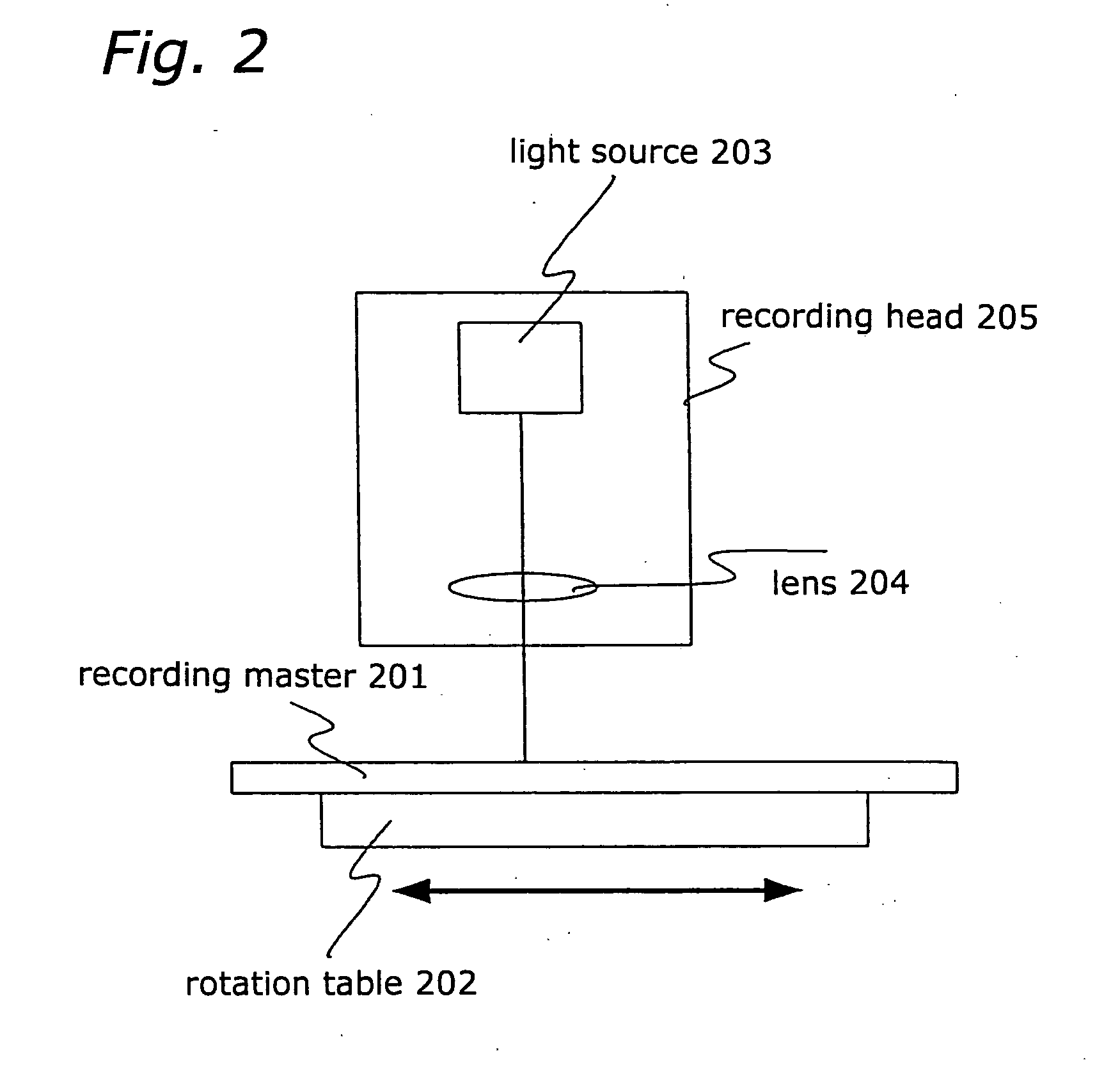
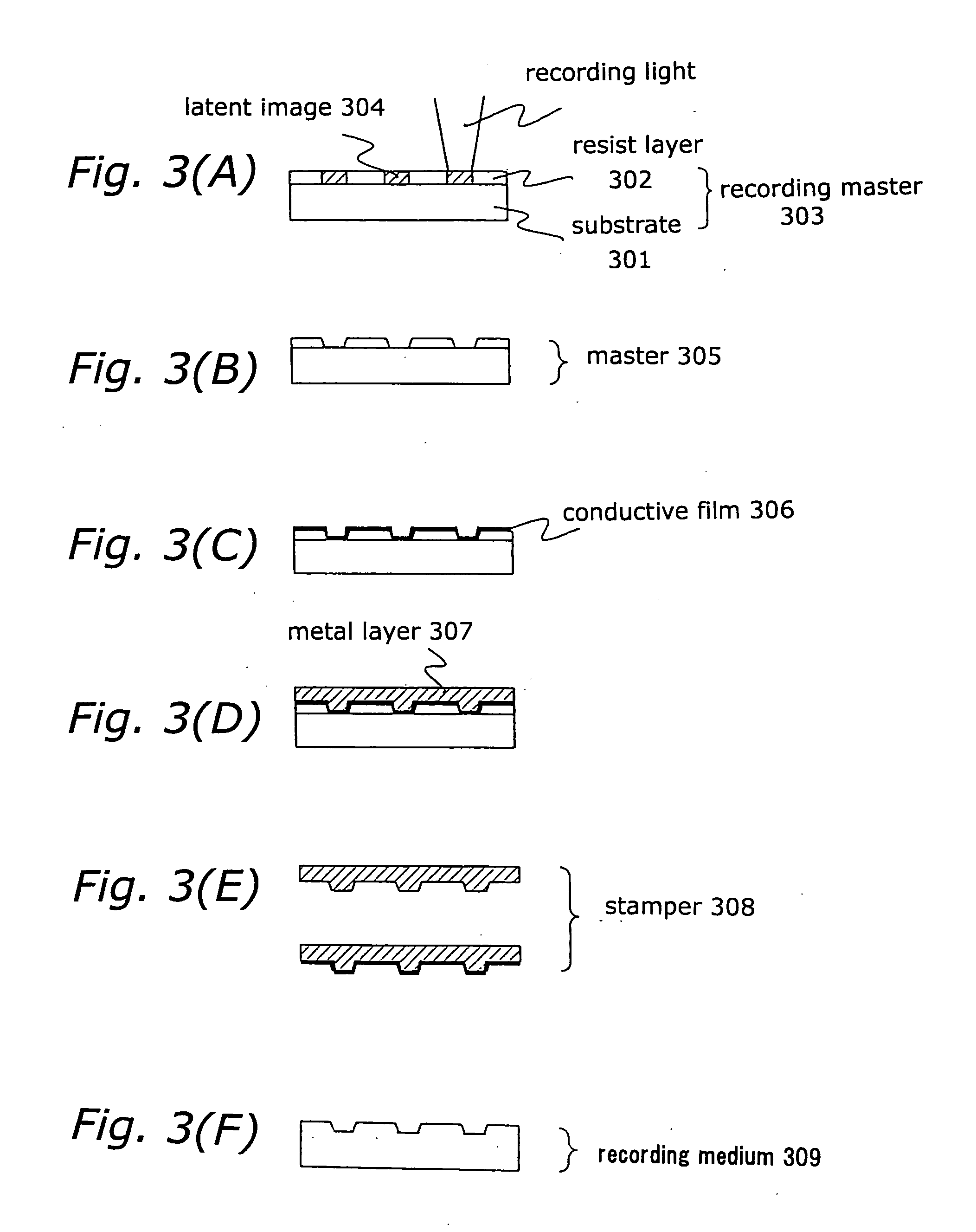
[0057] Next, a method for manufacturing an optical information recording medium by using the resist and the method for forming a pattern of the present invention will be described with reference to more detailed data. Note that, steps previous to manufacturing the master of an optical information recording medium are as described above, and the following description is only an example of the above method. The following description does not limit the range of application of the method of the present invention. A resist of TeOxPdy was formed to a thickness of 60 nm on a substrate made of quartz glass having diameter 200 mm and thickness 5 mm. The resist was formed by using a target that is a mixture of Te and Pd at the ratio of 74 to 26 and a gas mixture of Ar and O by the reactive sputtering method, so as to make a recording master. Pressure inside the vacuum chamber was 2 mTorr during the sputtering, and partial pressure of O was 0.6 mTorr. Particularly good cha...


PUM

PropertyMeasurementUnit
wavelengthaaaaaaaaaa

Abstract

A method of manufacturing a master of an optical information recording medium includes a resist layer formation step of using a resist to form a resist layer on an upper surface of a substrate, an exposure step for selectively exposing the resist layer to cause a change of state in the resist layer, and a development step for performing an alkali development process on the resist layer after the exposure step. The resist is primarily composed of an inorganic material and contains at least Te and O, and further contains a stabilizing additive having a lower solubility than TeO2 in an alkaline environment.

Description

BACKGROUND OF THE INVENTION [0001] 1. Field of the Invention [0002] The present invention relates to a resist that enables heat-mode recording, a method for forming a pattern using the resist, a method for manufacturing an optical information recording medium, a master, a stamper, and an optical information recording medium. [0003] 2. Description of the Prior Art [0004] A method for forming a pattern uses a photosensitive material that is called a resist, in which the state of the resist changes selectively by means of exposure to light (including various radiation rays such as an electron beam or a charged particle beam). After that, etching (and developing) is performed so as to form a pattern of pits and lands by using different etching rates between portions where the state of the resist is changed and portions where the state is not changed. This method is practically used in various types of micromachining for manufacturing optical information recording media or semiconductor ...

Claims


Application Information

Patent Timeline
Patent Type & Authority Applications(United States)
IPC IPC(8): G03F7/004G11B7/26
CPCG03F7/0042G11B7/263G11B7/261G03F7/0043G11B7/26
Inventor ITO, EIICHIOHNO, EIJIKAWAGUCHI, YUUKO
Owner PANASONIC CORP
Why Eureka
Try Eureka