Optical element and optical add-drop module

a technology of optical elements and modules, applied in the field of optical elements and optical adddrop modules, can solve the problems of high cost, difficult control of the thickness of the film layer which constitutes the multi-layer film filter, and high production costs, and achieves excellent environmental resistance, low cost, and improved reliability.

Inactive Publication Date: 2005-01-27
SANTEC
View PDF15 Cites 28 Cited by
  • Summary
  • Abstract
  • Description
  • Claims
  • Application Information

AI Technical Summary

Benefits of technology

[0018] In order to solve the above-mentioned problems, one of the objectives of the present invention is to provide an optical element and an optical add-drop module, which can change wavelength selection characteristics at high speed.
[0021] In the present invention, since the spacer layer is made of a paraelectric material having the secondary electrooptic effect, hardly any hysteresis effects are generated. The hysteresis effects are generated by the primary electrooptic effect. With this arrangement, it becomes possible to set the center wavelength of the optical element, such as a tunable optical filter, with high precision, in response to an applied voltage, and also to control the center wavelength thereof.
[0023] As described above, in accordance with the present invention, by altering the film design, it is possible to realize an optical element having an optional passband width and a signal-eliminating characteristic for signals with the other wavelengths. Moreover, since the wavelength is changed by controlling the refractive index, it is possible to improve reliability without the necessity of installing any mechanical driving units. The optical element is also excellent in environment resistance. Moreover, by designing films, the optical element of the present invention makes it possible to achieve tunable optical filters having an optional passband width and a signal-eliminating characteristic for signals with other wavelengths, that is, various filters such as a lowpass filter, highpass filter, bandpass filter and notch filter. The present invention simply requires electrode terminals and circuit components to be used for controlling an applied voltage so that it is possible to form a tunable optical filter at low cost.
[0024] Furthermore, by altering the film designing using the optical element, it is possible to realize an optical add-drop module having an optional passband width and a signal-eliminating characteristic for signals with the other wavelengths. Since the wavelength is changed through refractive-index control, no mechanical driving parts are required, making it possible to improve the reliability. The present invention simply requires electrode terminals and circuit components for controlling an applied voltage, so that it is possible to form a tunable add-drop module at low cost.

Problems solved by technology

This is because, as the number of cavities increases to double, triple and so on, the film thickness control of each layer which constitutes the multilayer film filter becomes difficult.
Moreover, it is difficult to produce the filters with high yield, causing very high costs.
Therefore, even in an attempt to apply the tunable optical filter 101 to this OADM, there is a limitation in the response speed upon changing the wavelength to be added or dropped.
For this reason, although it is possible to meet a limited request such as a request for assigning a specific communication path to a specific customer during a predetermined time zone, it is impossible to dynamically select a wavelength to be added or dropped at a high speed.
Moreover, the filter properties are more susceptible to environmental influences such as humidity and temperature.
For this reason, it becomes difficult to obtain superior properties with respect to incident light with a high output.
An attempt to carry out a DC driving operation would cause a dielectric breakdown.
The resulting problem is that, although the tunable optical filter 121 is allowed to change the wavelength, it fails to maintain the wavelength in a fixed state within a desired filter wavelength.
Moreover, with respect to optical add-drop modules which add and drop optical signals by using tunable optical filters also, conventionally, the same problems have been raised.

Method used


Image

  • Optical element and optical add-drop module
  • Optical element and optical add-drop module
  • Optical element and optical add-drop module

Examples


first embodiment

[0070] (First Embodiment)

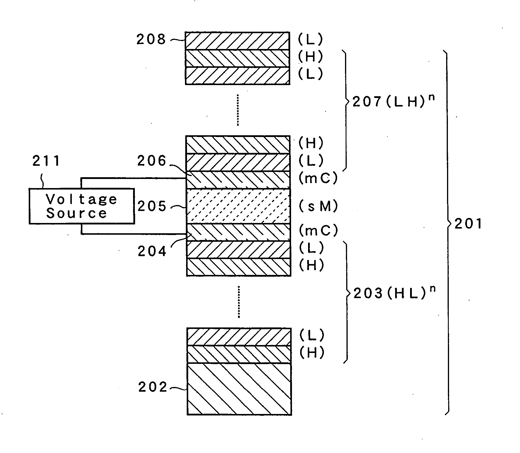
[0071] Next, the following description will discuss a first embodiment of the present invention. FIG. 4 shows the outline of the structure of an optical element 201 in accordance with of the first embodiment of the present invention. This optical element 201 has a structure in that a first mirror stack layer 203 is formed on a substrate 202 with a first conductive thin film 204 being formed thereon. The layer 203 and film 204 constitute a first composite stack layer. Then, a spacer layer 205, which is a paraelectric layer that exerts a secondary electrooptic effect, is formed thereon. Moreover, a second composite stack layer, constituted by a second conductive thin film 206 and a second mirror stack layer 207, is formed thereon. A coupling layer 208 is further formed thereon to form a basic structure. The coupling layer 208 (low-refractive index dielectric thin film L forming the uppermost layer), located on the second mirror stack layer 207, is made in cont...

second embodiment

[0105] (Second Embodiment)

[0106] The following description will discuss the embodiments of the present invention by exemplifying cases in which the optical element is practically applied to a bandpass filter.

[0107]FIG. 5 shows the structure of a tunable etalon in accordance with a second embodiment of the present invention theoretically. Here, the etalon is an optical element in which an illuminator is formed on the inside of an optical flat. A tunable etalon 301 of the present embodiment may be used as, for example, a tunable optical filter, and has its design wavelength λ0 of 1550 nm.

[0108] The tunable etalon 301 has a structure in that each of first and second composite stack layers 302 and 303 is joined to each of two surfaces of a spacer layer 304. Here, the first composite stack layer 302 has a structure in that: a first mirror stack layer 3121 is laminated on a BK7 glass substrate 3111 made of borosilicate glass; a transparent conductive film 3131 is vapor deposited on the ...

third embodiment

[0121] (Third Embodiment)

[0122]FIG. 8 shows the cross-sectional structure of a single cavity-type tunable bandpass filter with no electrode attached thereto, in accordance with the third embodiment of the present invention. A single cavity-type tunable bandpass filter 401 has a structure in that a first mirror stack layer 4111 is formed on aBK7 glass substrate 402. With respect to the first mirror stack layer 4111, a Ta2O5 film is used as a dielectric thin film 403, that is, the high-refractive index dielectric thin film H, and an SiO2 film is used as the low-refractive index dielectric thin film L, and seven sets of these films are laminated (in the figure, only two sets are briefly shown). An ITO film (refractive index: nc=2.0) is formed as a transparent conductive film 4121 on the stack layer 4111. The transparent conductive film 4121 serves as a transparent film in the vicinity of a wavelength of 500 nm, and has resistivity of 4×10⁻⁴ Ωcm.

[0123] A spacer layer 413 is formed on t...


PUM

PropertyMeasurementUnit
thicknessaaaaaaaaaa
thicknessaaaaaaaaaa
thicknessaaaaaaaaaa

Abstract

In an optical element, a first mirror stack layer is formed on a substrate, and a spacer layer made of a paraelectric material having a secondary electrooptic effect is formed thereon through a first conductive thin film. Further, a second mirror stack layer is formed thereon through a second conductive thin film, and a coupling layer is formed thereon; thus, a basic structure of the optical element is formed. By changing a voltage to be applied between the first and second conductive thin films, it becomes possible to switch wavelengths of light to be transmitted through the optical element at a high speed.

Description

BACKGROUND OF THE INVENTION [0001] 1. Field of the Invention [0002] The present invention relates to an optical element and an optical add-drop module using such a filter, and more particularly, to an optical element capable of selectively transmitting or reflecting light having a specific wavelength while optionally changing the wavelength itself, and an optical add-drop module which has modularized these devices. [0003] 2. Discussion of the Related Art [0004] Optical bandpass filters have been used for selecting light with a specific wavelength from inputted light rays. Among the bandpass filers, a tunable optical filter capable of changing a wavelength to be selected is applied various cases. For example, the tunable filter is used as a component of a multi-channel analyzer so as to change the wavelength to measure properties of a substance. The typical application has been proposed in JP-A 08-227014 (1996). This tunable optical filter has realized tunable characteristic by chang...

Claims


Application Information

Patent Timeline
Patent Type & Authority Applications(United States)
IPC IPC(8): G02F1/03G02B5/28G02F1/055G02F1/21G02F1/31
CPCG02B5/284G02F2001/213G02F1/21G02B5/288G02F1/213
Inventor UEHARA, NOBORU
Owner SANTEC
Why Eureka
Try Eureka